This report presents a brief introduction to OLED (organic light emitting diode) and technologies available for top emission OLED. A detailed taxonomy for OLED is presented covering parts of the type of OLED, material used, manufacturing, applications among others. A detailed landscape analysis of patent and non-patent literature is done with a focus on Top Emission OLED (TEOLED). The product information of major players in the market is also captured for OLED. The final section of the report covers the existing and future market predictions for OLED.
Introduction
- OLED technology was firstly developed in 1987 at Eastman Kodak Company by Tang and Van Slyke using small-molecule (sm-OLED). In 1990 Richard Friend, Jeremy Burroughes and Donal Bradley discovered electroluminescence capabilities from conjugated polymers so laying down the foundations for a new generation of flat panel displays.
- The growing number of electronic devices using organic light emitting diode displays shows that after years of promise, the technology is increasingly finding place in many products. But while OLED displays might challenge LCDs as the screens of choice for smaller gadgets, the technology may not become mainstream for notebook PCs or TVs within this decade.
- OLED displays use organic compounds that emit light when exposed to an electric current. They are brighter, have better contrast, offer wider viewing angles, use less power, and provide faster response times than liquid crystal displays. OLED screens' thickness is a third of that of LCDs, since they don't need a back-light, and that makes them a good fit for portable electronics devices.
Read More?
Click on OLED Background to read more about OLED.
Traditional light bulbs were invented more than 130 years ago. Since then the basic principle of creating light remains the same, although the design has been tweaked.An electric current passing through a tungsten wire causes it to heat up and glow white hot.Today, more than 20% of electricity used in US buildings is eaten up by lights and nearly half that amount is used by traditional, incandescent light bulbs. It has been a long-term goal of scientists to come up with something that would reduce this mammoth energy demand.
The OLEDs do not heat up like today's light bulbs and so are far more energy efficient and last longer.They also produce a light that is more akin to natural daylight than traditional bulbs. The new polymer uses a fluorescent blue material instead which lasts much longer and uses less energy.
Top Emission OLED: Search Strategy
The present study on the IP activity in the area of OLED with focus on Top Emission OLED (TEOLED) is based on a search conducted on Micropat.
Control Patents
| |
|
|
|
|
| |
|
|
Global OLED Technology LLC | Top-Emitting OLED Device With Light-Scattering Layer and Color-Conversion. |
| |
|
|
Novaled AG | Top Emitting, Electroluminescent Component With Frequency Conversion Centres. |
| |
|
|
Eastman Kodak Company | Organic Light Emitting Diode With Improved Light Emission Through The Cathode. |
| |
|
|
Eastman Kodak Company | Method Of Manufacturing a Top-emitting OLED display Device with Desiccant Structures. |
| |
|
|
TPO Displays Corp. | Top-Emitting Organic Electroluminescent Display |
| |
|
|
Industrial Technology Research Institute | Method for Manufacturing a Pixel Array of Top Emitting OLED. |
| |
|
|
Samsung Corp. | Top Emission Organic Light Emitting Diode Display Using Auxiliary Electrode to Prevent Voltage Drop of Upper Electrode and Method of Fabricating the Same. |
| |
|
|
Global OLED Technology LLC | Method of Making a Top-Emitting OLED device having Improved Power Distribution |
| |
|
|
Fed Corp. | Top Emitting OLED with Refractory Metal Compounds as Bottom Cathode . |
| |
|
|
Emagin Corp. | Low Absorption Sputter Protection Layer for OLED Structure. |
Patent Classes
| |
|
|
| |||||||||||
| |
257/40 | USPC | Active solid-state devices (e.g., transistors, solid-state diodes) /Organic semiconductor material | |||||||||||
| |
257/E51.018 | USPC | Active solid-state devices (e.g., transistors, solid-state diodes) / organic solid state devices, processes or apparatus peculiar to manufacture or treatment of such devices or of parts thereof / structural detail of device / light-emitting organic solid-state device with potential or surface barrier | |||||||||||
| |
257/E51.019 | USPC | Active solid-state devices (e.g., transistors, solid-state diodes) / organic solid state devices, processes or apparatus peculiar to manufacture or treatment of such devices or of parts thereof / structural detail of device / light-emitting organic solid-state device with potential or surface barrier / Electrode | |||||||||||
| |
257/E51.02 | USPC | Active solid-state devices (e.g., transistors, solid-state diodes) / organic solid state devices, processes or apparatus peculiar to manufacture or treatment of such devices or of parts thereof / structural detail of device / light-emitting organic solid-state device with potential or surface barrier / Electrode / Encapsulation | |||||||||||
| |
257/E51.021 | USPC | Active solid-state devices (e.g., transistors, solid-state diodes) / organic solid state devices, processes or apparatus peculiar to manufacture or treatment of such devices or of parts thereof / structural detail of device / light-emitting organic solid-state device with potential or surface barrier / Electrode / Arrangements for extracting light from device (e.g., Bragg reflector pair) | |||||||||||
| |
257/E51.022 | USPC | Active solid-state devices (e.g., transistors, solid-state diodes) / organic solid state devices, processes or apparatus peculiar to manufacture or treatment of such devices or of parts thereof / structural detail of device / light-emitting organic solid-state device with potential or surface barrier / Multicolor organic light-emitting device (OLED) | |||||||||||
| |
313/504 | USPC | Electric lamp and discharge devices/solid-state type/ with particular phosphor or electrode material / Organic phosphor | |||||||||||
| |
H01L 27/28 | IPC | Semiconductor devices; electric solid state devices not otherwise provided for / devices consisting of a plurality of semiconductor or other solid-state components formed in or on a common substrate / including components using organic materials as the active part, or using a combination of organic materials with other materials as the active part | |||||||||||
| |
H01L 27/32 | IPC | Semiconductor devices; electric solid state devices not otherwise provided for / devices consisting of a plurality of semiconductor or other solid-state components formed in or on a common substrate / including components using organic materials as the active part, or using a combination of organic materials with other materials as the active part / with components specially adapted for light emission, e.g. flat-panel displays using organic light-emitting diodes | |||||||||||
| |
H01L 51/50 | IPC | Semiconductor devices; electric solid state devices not otherwise provided for / solid state devices using organic materials as the active part, or using a combination of organic materials with other materials as the active part; processes or apparatus specially adapted for the manufacture or treatment of such devices, or of parts thereof / specially adapted for light emission, e.g. organic light emitting diodes (oled) or polymer light emitting devices (pled) | |||||||||||
| |
H01L 51/52 | IPC | Semiconductor devices; electric solid state devices not otherwise provided for / solid state devices using organic materials as the active part, or using a combination of organic materials with other materials as the active part; processes or apparatus specially adapted for the manufacture or treatment of such devices, or of parts thereof / Details of devices | |||||||||||
| |
H01L 51/56 | IPC | Semiconductor devices; electric solid state devices not otherwise provided for/specially adapted for sensing infra-red radiation, light, electromagnetic radiation of shorter wavelength, or corpuscular radiation; specially adapted either for the conversion of the energy of such radiation into electrical energy or for the control of electrical energy by such radiation / Processes or apparatus specially adapted for the manufacture or treatment of such devices or of parts thereo | |||||||||||
Concept Table
| S. No. | Concept 1 | Concept 2 | |
| |
| ||
| |
top emitting | oled | |
| |
top emissive | polymer led | |
| |
top emission | light emitting polymer diode | |
| |
toled | organic led | |
| |
teoled | organic electroluminescent diode | |
| |
foled | ||
| |
sm-oled | ||
| |
small molecule oled | ||
| |
amoled | ||
| |
pmoled | ||
Micropatent Search Strategy
Database: Micropat
Patent coverage: US, EP, WO, JP, DE, GB, FR
Time line: 1836/01/01 to 2011/02/20
| |
|
|
|
|
| |
Classes - OLED | Any Classification | H01L005150* OR H01L005152* OR H01L005156 OR H05B003308P OR 257E51.022 | 63152 |
| |
Classes - Organic Semiconductor Devices | Any Classification | 313504 OR 257040 OR 257E51.018 OR 257E51.019 OR 257E51.020 OR 257E51.021 OR H01L002728 OR H01L002732 | 27601 |
| |
Top Emission keywords | Claims, Title or Abstract | ((top emitting) OR (toled) OR (teoled) OR (te-oled) OR (top ADJ2 emitting) OR (top ADJ2 emissive) OR (top ADJ2 emission)) ADJ ((light ADJ emitting ADJ polymer) OR (organic ADJ electro-luminescence ADJ diode) OR (ORganic ADJ electroluminescent ADJ diode) OR (ploymer ADJ light ADJ emitting ADJ diode) OR (ORganic ADJ light ADJ emitting ADJ device) OR (self-luminous ADJ diode) OR (oled) OR (organic led arrays) OR (organic ADJ light ADJ emitting ADJ diode) OR (organic ADJ light ADJ emission ADJ diode) OR (polymer ADJ light ADJ emission ADJ device) OR (organic ADJ electroluminescent device) OR (oel) OR (oleds)) | 1141 |
| |
OLED keywords | Claims, Title or Abstract | ((organic OR (small adj molecule*1) OR polymer*1) adj (lightemitting OR (light adj (emitting OR emission)) OR electroluminescen*2 OR (electro adj luminescen*2))) NEAR3 diode*1) OR oled*2 OR smled*2 OR pled*2 OR (light adj (emitting OR emission) adj polymer*1) OR ((organic OR (small adj molecule*1) OR polymer*1) NEAR3 led*2) | 39392 |
| |
Top emissioin OLED keywords | Claims, Title or Abstract | (((((organic OR (small ADJ molecule*1) OR polymer*1) ADJ (lightemitting OR (light ADJ (emitting OR emission)) OR electroluminescen*2 OR (electro ADJ luminescen*2))) NEAR3 diode*1) OR oled*2 OR smled*2 OR pled*2 OR (light ADJ (emitting OR emission) ADJ polymer*1) OR ((ORganic OR (small ADJ molecule*1) OR polymer*1) NEAR3 led*2)) AND ((top ADJ3 (emissi*2 OR emitting)))) OR (te ADJ oled*2) | 429 |
| |
Top Emission keywords AND OLED classes | Combined query | 1 AND 3 | 809 |
| |
LED Keywords | Claims, Title or Abstract | ((lightemitting OR (light ADJ (emitting OR emission)) OR electroluminescen*2 OR (electro ADJ luminescen*2)) NEAR3 diode*1) OR led*2 OR oled*2 OR smled*2 OR pled*2 | 1617014 |
| |
Top emission keywords AND Organic semiconductor devices classes AND Top emission keywords | Combined query | 2 AND 7 AND 3 | 224 |
| |
Top emissioin OLED keywords | Full patent spec. | (((((organic OR (small ADJ molecule*1) OR polymer*1) ADJ (lightemitting OR (light ADJ (emitting OR emission)) OR electroluminescen*2 OR (electro ADJ luminescen*2))) near3 diode*1) OR oled*2 OR smled*2 OR pled*2 OR (light ADJ (emitting OR emission) ADJ polymer*1) OR ((organic OR (small ADJ molecule*1) OR polymer*1) near3 LED*2)) near3 ((top ADJ3 (emissi*2 OR emitting)))) OR (te ADJ oled*2) | 1506 |
| |
German Keywords | Full patent spec. | ((top adj3 (emissi*2 OR emitting)) OR (Top NEAR2 emittierende*1)) NEAR3 ((organische NEAR2 (led*1 OR Leuchtdiode*1)) OR (Licht adj emittierende adj Polymer*1) OR oled*1) | 1430 |
| |
French Keywords | Full patent spec. | ((top ADJ3 (émissive OR émettant)) OR (démission ADJ top) OR (top ADJ3 (emissi*2 OR emitting))) NEAR3 ((diode*1 NEAR3 électroluminescente NEAR3 organique*1) OR ((Polymère*1 OR organiques) ADJ2 led*1) OR (polymère*1 NEAR3 émettant NEAR3 lumière) OR oled*1) | 1412 |
| |
Combined query | 5 OR 6 OR 8 OR 9 OR 10 OR 11 | 2113 (1132 unique) | |
| |
Control Patents | Patent/Publication No. | WO2001057904A1 OR EP1029336A1 OR EP1489671A2 OR US20050236629A1 OR US20060043373A1 OR US20080169757A1 OR US6770502B2 OR US7002293B2 OR US7781961B2 OR US7791271B2 | 10 |
| |
Combined query | 12 AND 13 | 10 |
Scientific Literature Search
| |
|
|
|
|
| |
Google scholar | (Top emitting or top emission or top emissive) and ((organic light emitting diode) or (polymer led) or (light emitting polymer led) or (OLED)) | 1990-2011 | 1840 |
Search in Japanese database
Database: IPDL (Industrial property digital library), Japan
Date of search: 1900/01/01 to 2011/02/15
| |
|
|
|
|
| |
1900/01/01 to 2011/03/02 | 3K107 | DD03*[AA01+BB01+BB02+BB03+BB04+BB05+BB06+BB07+BB08+DD01+DD04+DD42+DD50+CC01+CC02+CC04+CC06+CC07+ CC08+CC09+EE02+EE03+EE06+EE22+GG01+GG02+GG03+GG04+GG05+GG06+GG07+GG08+GG08] |
1596 |
- F-Terms and theme used in search
| |
| ||
| |
F- Term theme | 3K107 | Electroluminescent light sources |
| |
F- Term | AA01 | Organic electroluminescent element. |
| |
F- Term | BB01 | Used in displays. |
| |
F- Term | BB02 | Used in Lights or light sources |
| |
F- Term | BB03 | Used in Backlights or the like for liquid crystals |
| |
F- Term | BB04 | Used in printer heads |
| |
F- Term | BB05 | Used in lasers |
| |
F- Term | BB06 | Used in designs or advertisements |
| |
F- Term | BB07 | Used in timepieces |
| |
F- Term | BB08 | Used in on-board use |
| |
F- Term | DD01 | Having feature of all direction of light emission. |
| |
F- Term | DD03 | Having top emission. |
| |
F- Term | DD04 | Having double sided emission. |
| |
F- Term | DD42 | Having Organic materials. |
| |
F- Term | DD50 | Structured with Light emitting layers |
| |
F- Term | CC01 | Having Light emitting layers |
| |
F- Term | CC02 | Light emission characteristics were improved. |
| |
F- Term | CC04 | Has an effect on brightness. |
| |
F- Term | CC06 | Has an effect on efficiency |
| |
F- Term | CC07 | Has an effect on colours. |
| |
F- Term | CC08 | Has an effect on Colour purity; Colour temperatures; Light emission wavelengths, including UV |
| |
F- Term | CC09 | Has colour balance feature |
| |
F- Term | EE02 | Has white light emission. |
| |
F- Term | EE03 | Display having Passive matrices |
| |
F- Term | EE06 | Display having Active matrices |
| |
F- Term | EE22 | Display having with RGB picture elements having different areas |
| |
F- Term | GG01 | Dispaly having color filters. |
| |
F- Term | GG02 | Apparatus for deposition |
| |
F- Term | GG03 | Apparatus for dry methods |
| |
F- Term | GG04 | Apparatus for chemical vapour deposition |
| |
F- Term | GG05 | Apparatus for evaporation |
| |
F- Term | GG06 | Apparatus for sputtering |
| |
F- Term | GG07 | Apparatus for wet methods |
| |
F- Term | GG08 | Apparatus for printing |
| |
F- Term | GG08 | Apparatus for Inkjet |
Taxonomy
Sample Analysis
Patent Analysis
A sample of 200 patents from the search is analyzed based on the taxonomy. Provided a link below for sample spread sheet analysis for Top Emission OLED.
| |
|
|
|
|
|
| |||||||
| |
|
|
Samsung Mobile Display Co., Ltd. | Top-emitting organic light emitting device | In the conventional top-emitting organic light emitting device, each pixel electrode is designed to have a minimum width, and neighboring pixel electrodes are designed to be widely spaced apart from each other by as much as 17 .mu.m. Therefore, the wide space between the pixel electrodes leaks emitted light, thereby deteriorating the voltage-current characteristics of the thin film transistors i.e., increasing photo-leakage. | In this patent the top-emitting organic light emitting device has maximized the width of a pixel electrode , thereby enhancing aperture ratio. Furthermore, the pixel electrode is arranged to overlap all thin film transistors, so that light is prevented from leaking through a space between neighboring pixel electrodes, thereby reducing photo-leakage of the thin film transistor. | |||||||
| |
|
|
Sanyo Electric Co., Ltd. | Light emitting display apparatus having excellent color reproducibility | Organic electroluminescence panel obtains white light by synthesizing two lights each having complementary color to the other, and the three primary colors differ in luminous intensity. Therefore it is difficult to set chromaticity of white light to desired level. And even after color-filter transmission, red light and blue light will have stronger luminous intensity than green light. | The present invention objective provide a light emitting display apparatus having excellent color reproducibility. Organic light emitting layer that synthesizes two or more complementary colors of light that are complementary to each other thereby producing white light. It has a resonant structure by which a resonant wavelength is set to a predetermined wavelength, and outputs the white light via the resonant structure where the predetermined wavelength substantially coincides with a wavelength corresponding to a primary color whose luminous intensity is uniform.With the stated construction, non-uniformity in luminous intensity among three primary colors is alleviated by means of amplified luminous intensity due to resonance. This will help obtain white light in which the primary colors are balanced well. | |||||||
| |
|
|
Canon Kabushiki Kaisha | Organic luminescence device with anti-reflection layer and organic luminescence device package | In organic luminescence device, the transparent electrode is formed by a material of a refractive index higher than that of air or nitrogen, constituting the external environment of the organic luminescence device. Therefore, the light emitted from the light emitting layer is reflected at a light emitting surface of the transparent electrode , namely at the interface between the transparent electrode and the air constituting the external environment in FIG. 1. For this reason, such organic luminescence device has been associated with a low efficiency of light emission to the exterior. | The present invention is to provide an organic luminescence device of a high light-emitting efficiency to the exterior and an organic luminescence device of a satisfactory contrast. A case holding the organic luminescence device in an internal holding space, in which a light emitted from the organic luminescence device, is emitted to the exterior through a light emitting side of the case; wherein anti-reflection means is provided on a light-emitting face on the light-emitting side among faces constituting the internal holding space of the case | |||||||
| |
|
|
Eastman Kodak Company | Integrated touch screen and OLED flat-panel display | It has the problem of multiple external electrical connections by employing a flat-panel display having a substrate that extends beyond the substrate of the resistive touch screen. | The present invention has the advantage that it reduces the costs and improves the reliability and performance of a touch screen that is used with an OLED flat-panel display by integrating cable connections on a single substrate and providing touch screen signal processing on the display substrate. | |||||||
| |
|
|
FED Corporation | Passive matrix OLED display | The disadvantage of oxygen and moisture penetration into the interior of the organic light emitting device is the potential to form metal oxides at the metal-organic interface. These metal oxide impurities may allow separation of the cathode or anode and the organic in a matrix . This can result in the formation of dark non-emitting spots (i.e., no illumination).Edge shorting between the cathode and anode layers is a current problem affecting most conventional organic light emitting display devices. This edge shorting reduces the illuminating potential of the display devices. | The present invention to provide an insulator layer to minimize edge shorts between lines by separating the OLED layer and the electrode elements. It also provides a sealing structure to isolate the OLED layer from moisture and other contaminants. | |||||||
| |
|
|
None | ORGANIC LIGHT EMITTING DIODE DISPLAY AND METHOD OF MANUFACTURING THE SAME | In the organic light emitting layer, as it is easy to transfer energy in an interface between a light emitting layer and a hole transfer layer, a light emitting efficiency and lifetime of the OLED display are reduced because of an energy loss of triplet inside the OLED display. | An interface of the light emitting layer can be improved by forming the inorganic oxide layer between the hole transport layer and the light emitting layer. Further, an energy loss of triplet can be prevented, and the emission efficiency and lifetime can be improved. | |||||||
| |
|
|
Samsung Electronics Co., Ltd. | Manufacturing flat panel displays with inkjet printing systems | For manufacture of certain flat panel display devices, such as LCDs or OLED displays, various thin film patterns are formed on panel substrates of the devices, typically using photolithography processes. However, as displays become larger, the amount of material that must be deposited on substrates to form the thin film patterns also becomes larger, inturn increases the manufacturing costs of the panels. | Inkjet printing systems have been developed for forming the thin film patterns on the substrates by depositing them on the substrates in the form of special inks. These systems deposit the ink on the substrate through an inkjet head. However, the inkjet head includes a plurality of nozzles, and if only one of these nozzles becomes dysfunctional, the number of passes that the inkjet printing head must make increases. As a result, processing time and costs are substantially increased. | |||||||
| |
|
|
Eastman Kodak Company | Device for depositing patterned layers in OLED displays | To achieve color pixelation in OLED imaging panels, fabrication of a multicolor OLED imaging panel using a shadow masking method is used. A multicolor organic electroluminescent ("EL") medium is vapor deposited and patterned by controlling an angular position of a substrate with respect to a deposition vapor stream. The positioning an element in direct contact with a surface of a substrate can invite problems of abrasion, distortion, or partial lifting, this may cause abrasion, distortion, or partial lifting of the first-color pattern. | The present invention is that a pattern of vaporized material, such as organic material, can be deposited without the use of shadow mask.Another feature is that a plurality of devices can be used for simultaneously depositing different organic materials. Such organic materials can emit light in different ranges of the spectrum. | |||||||
| |
|
|
AU Optronics Corp. | Driving method for active matrix OLED display | In one display frame, the current received by the OLED is fixed.The driving method used previously accumulates carriers inside the OLED which reduce the life of the OLEDs. Moreover, the voltage across the OLED gradually increases over timewhich inturn increases power. This effects the OLED over time. | The present invention uses a driving method to neutralize carrier accumulation in the OLED, thereby reducing the increase in voltage and minimizing the increase in power consumption across both ends of the OLED over time, further increasing the life of the OLED. | |||||||
| |
|
|
Eastman Kodak Company | Depositing layers in OLED devices using viscous flow | To achieve color pixelation in OLED imaging panels, fabrication of a multicolor OLED imaging panel using a shadow masking method is used. A multicolor organic electroluminescent ("EL") medium is vapor deposited and patterned by controlling an angular position of a substrate with respect to a deposition vapor stream. The positioning an element in direct contact with a surface of a substrate can invite problems of abrasion, distortion, or partial lifting, this may cause abrasion, distortion, or partial lifting of the first-color pattern. | The present invention is that the method of color pixelating an organic layer includes providing a plurality of vapor sources disposed outside of a deposition chamber for generating vapors of organic materials, and connecting such vapor sources to a manifold disposed in the chamber. By using vapor deposition method, we can eliminate precision shadow masks. | |||||||
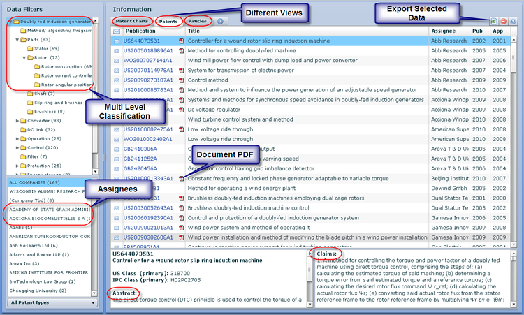
Click here to view the detailed analysis sheet for doubly-fed induction generators patent analysis.
Article Analysis
| |
|
|
|
|
| |
| |
Application of Screen Printing in the Fabricationof Organic Light-Emitting Devices | Dino A. Pardo, Ghassan E. Jabbour,* andNasser Peyghambarian | 01/27/2000 | Optical Sciences Center, University of Arizona.IEEE 27 Jan 2000 | This article explains the screen printing technique which deposits organic active layer having a thickness of several tens of nanometers and acting as a hole-transport layer (HTL) in multilayer OLEDs. The resulting devices emitlight at low voltage (<5 V) and have a peak external quantum efficiency of 0.91 %. | |
| |
Multicolor Organic Light-Emitting DiodesProcessed by Hybrid Inkjet Printing | Shun-Chi Chang, Jie Liu, Jayesh Bharathan,Yang Yang,* Jun Onohara and Junji Kido | 08/07/1999 | Department of Materials Science and EngineeringUniversity of California at Los Angeles. willey 8 Jul 1999 | This article presents a multicolor patterning technique to produce controllable patterning of red-green-blue OLEDs with fine pixel displays. The LEDs comprise bilayer structures of red and green dopants with inkjet-printed onto a film of the blue-emitting semiconducting polymer, the latter serving as the hole-transport layer. | |
| |
Organic light-emitting diode (OLED)technology: materials, devices and displaytechnologies | Bernard Geffroy, Philippe le Roy and Christophe Prat | 06/02/2006 | Laboratoire Cellules et Composants. willey 6 Feb 2006 | This article presents an overview of OLED's over LCD's. OLED'S have a thickness, currently less than 2 mm. Having high contrast ratio is also a strong point of OLED and also in fast response time.OLEDs for flat-panel display applications are their self-emitting property, high luminous efficiency, full-colour capability, wide viewing angle, high contrast,low power consumption, low weight, potentially large area colour displays and flexibility. | |
| |
Organic/polymeric electroluminescent devices processed by hybrid ink-jet printing | Yang Yang, Shun-Chi Chang, Jayesh Bharathan and Jie Liu | 04/05/1999 | Journal of Materials Science: Materials in Electronics Volume 11, Number 2, | The HIJP concept is a unique approach for fabricating polymer and organic electronic devices. One is able to apply this technology for the deposition of various functional materials such as charge-injection layers, charge-blocking layers, and multicolor polymer/organic emissive layers. It can be used for the fabrication of logos, indicator lights, multicolor displays and also in bio-medical applications such as biosensors for low cost diagnostics. | |
| |
White Organic Light-Emitting Devices for Solid-State Lighting | B. W. D'Andrade, S. R. Forrest | 14/10/2004 | Department of Electrical Engineering, Princeton University Willey 14 OCT 2004 | This article presents the WOLEDs increasing display applications for use primarily as liquid-crystal display backlights. They have achieved high material purity, low cost, high brightness,color quality and long operational life-times. | |
| |
White organic light-emitting diodes with fluorescent tube efficiency | Sebastian Reineke, Frank Lindner, Gregor Schwartz, Nico Seidler, Karsten Walzer | 14/05/2009 | Institute of Applied Photophysics. Vol 459 Macmillan Pub | This article presents an WOLED havinh high internal quantum efficiencies for the con-version of electrical energy to light have been realized by focussing on reducing energetic and ohmic losses that occur during electron–photon conversion.This can be achieved by improved OLED structure which reaches fluorescent tube efficiency. By combining a care-fully chosen emitter layer with high-refractive-index substrates and using a periodic outcoupling structure | |
| |
Precision ink jet printing of polymer light emitting displays | J. F. Dijksman, P. C. Duineveld, M. J. J. Hack, A. Pierik, J. Rensen, J.-E. Rubingh, I. Schram andM. M. Vernhou | 09/11/2006 | Philips Research Laboratories RSC | Precision ink jet printing of organic polymer light emitting diodes relies strongly on the accuracy of the droplet generation process.Image capturing using one image at a time for image processing delivers sharper images and can be used for optically measuring droplet volumes. | |
| |
High-efficiency microcavity top-emitting organic light-emittingdiodes using silver anode | Huajun Peng, Jiaxin Sun, Xiuling Zhu, Xiaoming Yu, Man Wong, and Hoi-Sing Kwok | 17/02/2006 | Hong Kong Universityof Science and Technology. AIP | High efficient top-emitting OLEDs have been fabricated using highly reflective Ag as the anode. Surfacemodification of the Ag anode by CF4 plasma substantially enhances the hole injection efficiency. The color variation isalmost eliminated in the TOLED. The optimized microcav- ity TOLED has a current efficiency enhancement of 65% and a total outcoupling efficiency enhancement of 35%, as compared with a conventional OLED. | |
| |
Inverted top-emitting organic light-emitting diodes using transparent conductive NiO electrode | Se-W. Park, Jeong-M. Choi, Eugene Kim and Seongil Im | 09/01/2005 | Institute of Physics and Applied Physics, Applied Surface Science 244 (2005) 439–443 | TE-OLED device uses a thermally evaporated and semi-transparent NiO film as a top-electrode. Since the sheet resistance of our NiO was very high and its transmittance was only about 50%, the resulting luminance and injection current of our TE-OLED were much inferior to those of the BE-OLED device. | |
| |
Self-assembled monolayer-modified Ag anode for top-emitting polymerlight-emitting diodes | Lai-Wan Chong, Yuh-Lang Lee,a͒ and Ten-Chin Wenb͒ | 07/12/2006 | Department of Chemical Engineering, National Cheng Kung University | Self-assembled monolayer is a method to modify the Ag anodes for application in T-PLED. The Ag electrode can be utilized as an effective anode to improve the emitting characteristic of a T-PLED. The Ag anode enhances the hole injection, reduce the op-eration voltage, and significantly increase the current inten-sity and luminous efficiency of the device, without decreasing the reflectivity of the Ag anode. | |
Click here to view the detailed analysis sheet for Top Emission OLED for non patent literature
Top Cited Patents
| |
|
|
|
|
|
| |
US6096496A | |
Frankel; Robert D | Supports incorporating vertical cavity emitting lasers and tracking apparatus for use in combinatorial synthesis | |
| |
US6069443A | |
Fed Corporation | Passive matrix OLED display | |
| |
US6366017B1 | |
Agilent Technologies | Organic light emitting diodes with distributed bragg reflector | |
| |
US20020197511A1 | |
United Of America As Respresented By The Secretary Of The Air Force | High efficiency multi-color electro-phosphorescent OLEDS | |
| |
US6265820B1 | |
Emagin Corporation,De | Heat removal system for use in organic light emitting diode displays having high brightness | |
| |
US20020195968A1 | |
IBM | Oled current drive pixel circuit | |
| |
US20020186209A1 | |
Eastman Kodak Company | Touch screen for use with an OLED display | |
| |
US20030127973A1 | |
Universal Display Corporation | OLEDs having increased external electroluminescence quantum efficiencies | |
| |
US6844673B1 | |
Alien Technology Corporation | Split-fabrication for light emitting display structures | |
| |
US20040174116A1 | |
Universal Display Corporation | Transparent electrodes | |
| |
US20050194896A1 | |
Hitachi Displays Ltd. | Light emitting element and display device and illumination device using the light emitting element | |
| |
US20020074935A1 | |
Universal Display Corporation | Highly stable and efficient OLEDs with a phosphorescent-doped mixed layer architecture | |
| |
US20040217702A1 | |
Corning Incorporated | Light extraction designs for organic light emitting diodes | |
| |
US20020030647A1 | |
Universal Display Corporation | Uniform active matrix oled displays | |
| |
US20050248270A1 | |
Eastman Kodak Company | Encapsulating OLED devices | |
| |
US20040113875A1 | |
Eastman Kodak Company | Color oled display with improved power efficiency | |
| |
US20030230972A1 | |
Eastman Kodak Company | Oled display having color filters for improving contrast | |
| |
US20050040756A1 | |
Eastman Kodak Company | OLED device having microcavity gamut subpixels and a within gamut subpixel | |
| |
US6670772B1 | |
Eastman Kodak Company | Organic light emitting diode display with surface plasmon outcoupling | |
| |
US20040061136A1 | |
Eastman Kodak Company | Organic light-emitting device having enhanced light extraction efficiency | |
Top Cited Articles
Dolcera Dashboard
Dashboard Link
| Top Emission OLED - Dashboard |
- Flash Player is essential to view the Dolcera dashboard
Products
| |
|
|
| ||||||
| |
|
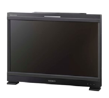 |
Digital Inputs Specifications | Detail: | |||||
| HDMI | HDMI (x1) (HDCP correspondence, Deep Color correspondence) | ||||||||
| SDI (SMPTE 259M) | BNC (x2) | ||||||||
| Display Specifications | Detail: | ||||||||
| Image Aspect Ratio | 16:09 | ||||||||
| Resolution | 1920 x 1080 pixels (Full HD) | ||||||||
| Screen Size | 24 5/8 inches (623.4 mm) | ||||||||
| Viewing Angle | 89°/89°/89°/89° | ||||||||
| General Specifications Specifications | Detail: | ||||||||
| Dimensions (W x H x D) | 22 3/4 x 16 3/4 x 5 7/8 inches | ||||||||
| Weight | 28 lb 11 oz | ||||||||
| Power Requirements Specifications | Detail: | ||||||||
| Power Consumption | Approx. 145 W | ||||||||
| Power Requirements | AC 100 V to 240 V, 1.6 A to 0.8 A, 50/60 Hz | ||||||||
| 2 | |
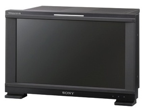 |
Digital Inputs Specifications | Detail: | |||||
| HDMI | HDMI (x1) (HDCP correspondence, deep colour correspondence) | ||||||||
| SDI | BNC (x2) | ||||||||
| Display Specifications | Detail: | ||||||||
| Image Aspect Ratio | 16:09 | ||||||||
| Resolution | 1920 x 1080 pixels (Full HD) | ||||||||
| Screen Size | 365.8 x 205.7 mm (14 1/2 x 8 1/8 inches) | ||||||||
| Viewing Angle | 89°/89°/89°/89° (typical) (up/down/left/right contrast >10:1) | ||||||||
| General Specifications Specifications | Detail: | ||||||||
| Dimensions (W x H x D) | 436.0 x 282.4 (266.4)* x 214.7 mm (17 1/4 x 11 1/4 (10 1/2)* x 8 1/2 inches) * Height without legs | ||||||||
| Weight | 8.5 kg (18 lb 11 oz) | ||||||||
| Power Requirements Specifications | Detail: | ||||||||
| Power Consumption | Approx. 65 W normally with input from a standard HDMI input. Approx. 115 W at maximum load, with four option slots in use and maximum luminance compensation for any deterioration due to aging. | ||||||||
| Power Requirements | AC 100 V to 240 V, 1.4 A to 0.7 A, 50/60 Hz DC 24 V to 28 V, 4.7 A to 4.0 A | ||||||||
| |
|
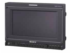 |
Digital Inputs Specifications | Detail: | |||||
| HDMI | Yes | ||||||||
| HDSDI (SMPTE 292M) | 3G/SDI/HDSDI | ||||||||
| SDI (SMPTE 259M) | Included | ||||||||
| Display Specifications | Detail: | ||||||||
| Back Light Technology | OLED | ||||||||
| Native Aspect Ratio | 16:09 | ||||||||
| Resolution | 960 x 540 | ||||||||
| Screen Size | Approx 7.4 inches | ||||||||
| Viewing Angle | 85°/85°/85°/85° (typical) (up/down/left/right contrast>10:1) | ||||||||
| General Specifications Specifications | Detail: | ||||||||
| Dimensions (W x H x D) | 8 7/8 x 7 1/4 x 6 3/8 inches Approx. 222.4 x 183.5 x 161.8 mm | ||||||||
| On-Screen Display | Yes | ||||||||
| Rack Mount | MB531 | ||||||||
| Weight | Approx. 5 lb 12 oz Approx. 2.6 kg | ||||||||
| Power Requirements Specifications | Detail: | ||||||||
| Power Consumption | Max. approx. 27W | ||||||||
| Power Requirements | AC 100 to 240 V 50/60 Hz 0.5A to 0.3A DC 12 V 1.9 A Rechargeable Battery Pack | ||||||||
Market Research
Major Players
| |
|
|
|
|
|
|
| |
UDC; Kodak; Add-Vision; Magin; Plextronics; Organic Lighting Technologies; GE;3M Innovation | CDT (Sumitomo Chemical) (UK); Novaled (G); Fraunhofer IPMS (G); OLED-T (UK); OTB (ND); MicroEmissive Displays (UK) | Seiko-Epson; Matsushita; Sony; Sumitomo Chemical; Sharp; TM Display; Konica –Minolta; Sanyo; Toppoly; Lumiotec; Canon; Toshiba | Samsung; LG Phillips LCD; Neo View; Doosan DND | AU Optoelectronics (AUO); Univision; Toppoly; Tetrahedron; Chi Mei Optoelectronics | |
| |
PPG; 3M; Dow Corning | Merck Materials (G); BASF (G); CDT (UK); Degussa/ Evonik (G); HC Starck (G); Sensient Imaging Technologies (G); Goodfellow Metals (UK); Novaled (G) | Sumitomo Chemical; Mitsubishi Chemical | Syndychem (Shenyang Syndy Chemistry Institute) | ||
| |
Corning; Rockwell Collins | ST Microelectronics (It, Fr); Infineon (G) | Maekawa; Matsushita; Toppoly | Dae Joo Electrncs | AUO; Richtek Technologies; Lightsonic; Univision; Wintek | Innocom Technologies Shenzen; RIT Display |
| |
eMagin; US Micro Products | Densitron Technologies (UK); MicroEmissive Displays (MED) (UK); Pacer International Distributors (UK reseller) | Seiko-Epson; Sharp; Sumitomo Chemical; Lumiotec; TMDisplay; Sanyo | Samsung SDI; Orion OLED; NeoView KOLON; Hyundai LCD | AUO; Chi Mei EL (CMEL); Univision Technology; Evervision Electronics; RiTDisplay; TPO Display | Visionix; Smartdisplays; Universal Display Technologoes (Jilin); Varitronix (HK); Blaze Display Technologies |
| |
OSD | Nokia; Sony-Ericsson | Sony; Matsushita; Hitachi; Toshiba; Imase | Samsung; LG Philips | ||
| |
GE | Thorn EMI (UK); OSRAM (G); Siemens (G) | Sumitomo Chemica |
source: Major players
SWOT analysis
| |
|
| • Capability for innovation • Production of base materials for OLED manufacture • Process equipment manufacture is easy. |
• Lack of industrial productive capacity or eco-system to support low-cost volume production • Capability to bring innovations to market – i.e. probability of export market success • Lack of branded consumer goods suppliers apart from mobile handsets – e.g. Nokia |
| |
|
| • Possible renaissance in manufacturing at low-cost • Use of IPR – with mitigations through agreements • Expansion in base materials supply and process equipment manufacture for low temperatures |
• Older technologies – TFT-LCDs which improve technically – become cheaper, flexible, lower power demands and better colour/contrast, scale up larger, etc, make existing (LCD) players far stronger • Strong competitive position and behaviour of current major players globally and market make market entry difficult or increasingly impossible |
Market Forecast
OLED Lighting Market Forecast
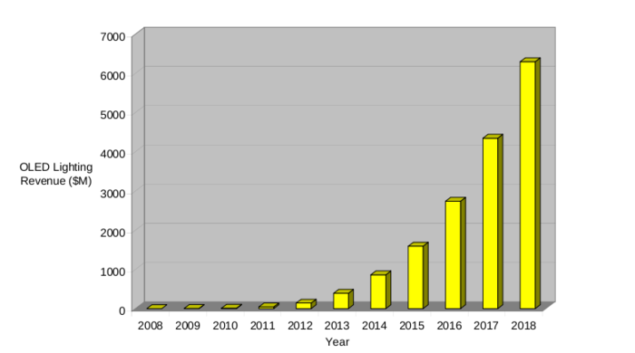
- OLED lighting will pick up in 2011, and reach $6.3B by 2018.
- The OLED lighting market will reach $1.5B by 2015, and $6.3B by 2018.
- Large investments have been made in OLED lighting in the EU, US, Japan and Korea.
- There are about 20 OLED lighting organizations worldwide. Europe is currently the leading participant in OLED lighting in terms of projects numbers, government funding, and participating companies.
- Over 100 companies and universities are currently working on OLED lighting.
OLED TV Market Forecast
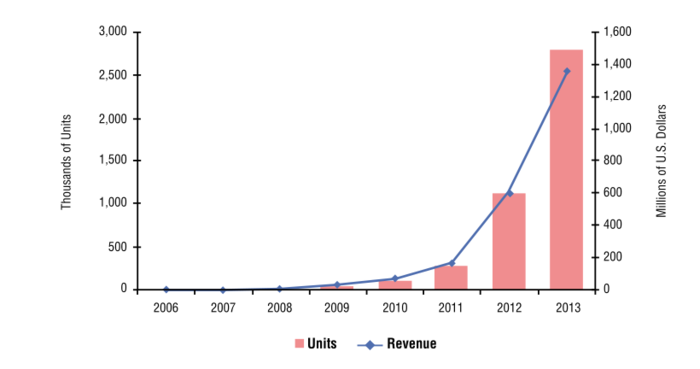
- OLED TV sets will account for around half of all revenue for OLED panels in 2012, growing rapidly from just $150 million in 2011 to $1.5 billion in 2013.
- iSuppli’s similarly forecasts the global OLED TV market will reach 2.8 million units by 2013, managing a compound annual growth rate (CAGR) of 212.3% from just 3,000 units in 2007.
- In terms of global revenue, OLED TV will hit $1.4 billion by 2013, increasing at a CAGR of 206.8% from $2 million in 2007.
OLED Dispaly Market Forecast
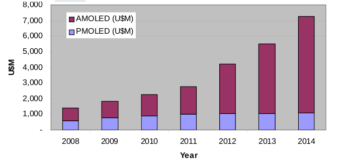
- OLED display market will grow to $5.5 billion by 2015, from $0.6 billion in 2008, with a CAGR of 37%. Currently, this growth is being driven by the adoption of active matrix OLED (AMOLED) displays for the primary display in mobile phones and portable media players.
Recent Licensing Activities in OLED Segment
| Licensor | Licensee | Date | Details |
| Global OLED Technology LLC | OLEDWorks | 6th Dec 2011 | Under the terms of the royalty-bearing license, OLEDWorks is granted the right to use certain GOT patents in connection with OLEDWorks’ commercialization of specified OLED lighting-related products. |
| Universal Display | Moser Baer | 8th Feb 2011 | Moser Baer agreed to license Universal’s OLED technology and purchase UniversalPHOLED (phosphorescent OLED) materials for white OLED panel manufacturing. The companies have agreed to work together for five years in the development of Moser Baer’s US-based OLED panel manufacturing project. |
| Universal Display | Pioneer Corp | 29th Sep 2011 | Pioneer is supposed to use Universal Display’s highly efficient, high-performance UniversalPHOLED® technology and materials for the manufacture and sale of OLED lighting products |
| DuPont | Samsung | 3rd Nov 2011 | Samsung needed new technology for its larger models for televisions and hoped to benefit from DuPont’s recent innovations. |
Landscape Analysis Of Top-Emmission OLED
Competitor Landscape
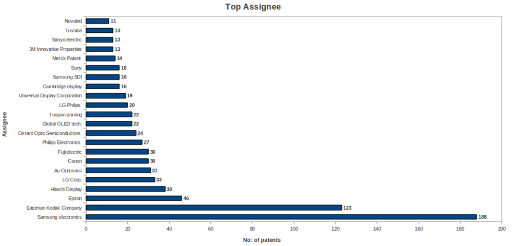
Top Assignee
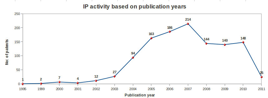
Filing trends over the publication years
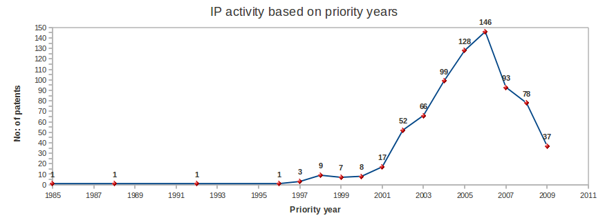
Filing trends over the priority years
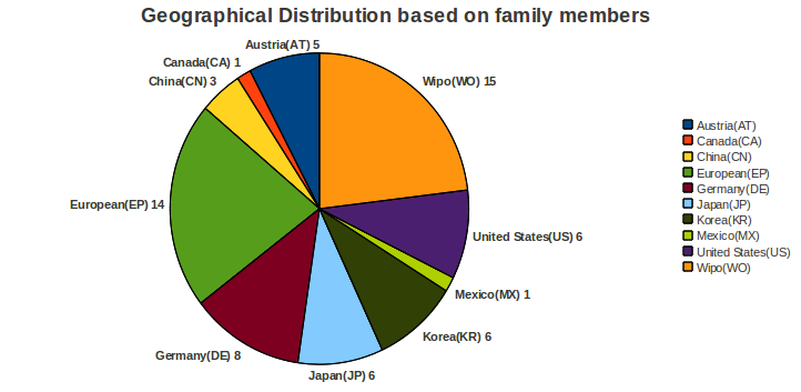
Geographical Distribution based on family members
- The geographical distribution is based on 10 sample patent numbers along with all their family members.
Key Inventor Mapping
| |
Inventor | 2000 | 2001 | 2002 | 2003 | 2004 | 2005 | 2006 | 2007 | 2008 | 2009 | 2010 | Total Result | |
| |
Cok, Ronald | 1
|
3
|
22
|
18
|
17
|
14
|
15
|
4
|
2
|
96
| |||
| |
Park, Jin Woo | 18
|
2
|
20
| ||||||||||
| |
Choi, Beohm Rock | 1
|
6
|
7
|
2
|
16
| ||||||||
| |
Kim, Nam Deog | 7
|
6
|
3
|
16
| |||||||||
| |
Tyan, Yuan Sheng | 2
|
7
|
3
|
1
|
1
|
1
|
15
| ||||||
| |
Winters, Dustin | 2
|
5
|
5
|
2
|
1
|
15
| |||||||
| |
Choi, Dong Soo | 13
|
1
|
14
| ||||||||||
| |
Choi, Joon Hoo | 2
|
3
|
4
|
5
|
14
| ||||||||
| |
Kwak, Won Kyu | 1
|
1
|
9
|
1
|
1
|
1
|
14
| ||||||
| |
Miller, Michael | 4
|
4
|
2
|
1
|
1
|
1
|
1
|
14
| |||||
| |
Park, Jae Yong | 2
|
8
|
4
|
14
| |||||||||
| |
Shore, Joel | 2
|
2
|
5
|
3
|
1
|
1
|
14
| ||||||
| |
Arnold, Andrew | 4
|
5
|
1
|
1
|
1
|
1
|
13
| ||||||
| |
Boroson, Michael | 1
|
4
|
3
|
1
|
4
|
13
| |||||||
| |
Goh, Joon Chul | 1
|
4
|
5
|
3
|
13
| ||||||||
| |
Tanaka, Masahiro | 1
|
1
|
1
|
5
|
4
|
1
|
13
| ||||||
| |
Choong, Vi En | 5
|
5
|
2
|
12
| |||||||||
| |
Ghosh, Amalkumar | 2
|
1
|
1
|
3
|
5
|
12
| |||||||
| |
Kim, Eun Ah | 1
|
2
|
9
|
12
| |||||||||
| |
Kobayashi Hidekazu | 1
|
2
|
2
|
5
|
1
|
1
|
12
| ||||||
| |
Total Result | 2
|
1
|
1
|
6
|
45
|
67
|
72
|
90
|
47
|
18
|
15
|
362
| |
Most Cited Patents
| |
|
|
|
|
| ||
| |
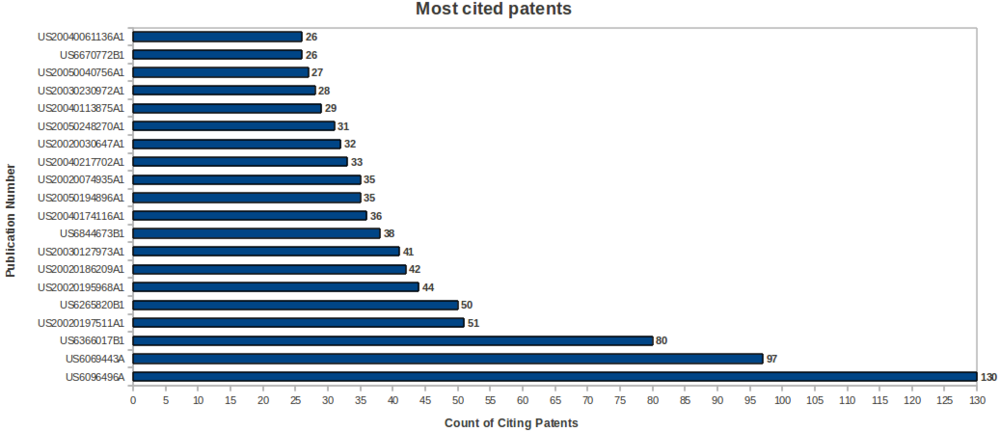
US6069443A | Fed Corporation | Passive matrix OLED display | 30/05/2000
|
| ||
| |
US6366017B1 | Agilent Technologies | Organic light emitting diodes with distributed bragg reflector | 02/04/2002
|
| ||
| |
US20020197511A1 | United Of America As Respresented By The Secretary Of The Air Force | High efficiency multi-color electro-phosphorescent OLEDS | 26/12/2002
|
| ||
| |
US6265820B1 | Emagin Corporation,De | Heat removal system for use in organic light emitting diode displays having high brightness | 24/07/2001
|
| ||
| |
US20020195968A1 | IBM | Oled current drive pixel circuit | 26/12/2002
|
| ||
| |
US20020186209A1 | Eastman Kodak Company | Touch screen for use with an OLED display | 12/12/2002
|
| ||
| |
US20030127973A1 | Universal Display Corporation | OLEDs having increased external electroluminescence quantum efficiencies | 10/07/2003
|
| ||
| |
US6844673B1 | Alien Technology Corporation | Split-fabrication for light emitting display structures | 18/01/2005
|
| ||
| |
US20040174116A1 | Universal Display Corporation | Transparent electrodes | 09/09/2004
|
| ||
| |
US20050194896A1 | Hitachi Displays Ltd. | Light emitting element and display device and illumination device using the light emitting element | 08/09/2005
|
| ||
| |
US20020074935A1 | Universal Display Corporation | Highly stable and efficient OLEDs with a phosphorescent-doped mixed layer architecture | 20/06/2002
|
| ||
| |
US20040217702A1 | Corning Incorporated | Light extraction designs for organic light emitting diodes | 04/11/2004
|
| ||
| |
US20020030647A1 | Universal Display Corporation | Uniform active matrix oled displays | 14/03/2002
|
| ||
| |
US20050248270A1 | Eastman Kodak Company | Encapsulating OLED devices | 10/11/2005
|
| ||
| |
US20040113875A1 | Eastman Kodak Company | Color oled display with improved power efficiency | 17/06/2004
|
| ||
| |
US20030230972A1 | Eastman Kodak Company | Oled display having color filters for improving contrast | 18/12/2003
|
| ||
| |
US20050040756A1 | Eastman Kodak Company | OLED device having microcavity gamut subpixels and a within gamut subpixel | 24/02/2005
|
| ||
| |
US6670772B1 | Eastman Kodak Company | Organic light emitting diode display with surface plasmon outcoupling | 30/12/2003
|
| ||
| |
US20040061136A1 | Eastman Kodak Company | Organic light-emitting device having enhanced light extraction efficiency | 01/04/2004
|
| ||
Most Cited Patents Mapping
Technology Mapping
- In OLED devices not all internally generated light is coupled out of the device (only 20%-50%), which reduces the device efficiency and lifetime.
- Modification in structures are applied to improve outcouple efficiency in order to enhance the efficiency and lifetime of top emission OLEDs.
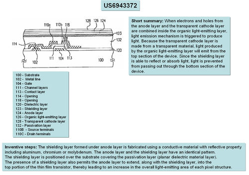
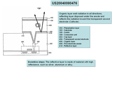
- Below is a snapshot of how various organizations are using different design structures, using the same principle of internal reflection, to achieve higher out-coupling efficiencies.
Comparison of out coupling of waveguiding light in top-emission polyLED stack
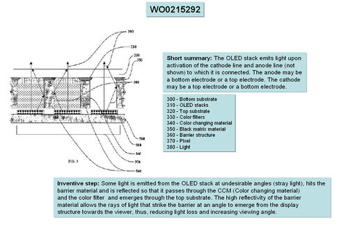
- Some light is reflected out of the OLED at stray angles in typical cases. By using a barrier material (form of microparticles) in the cathode layer, this light at stray angles hits the barrier material, and some of it is reflected back and guided out at the right angles, reducing light loss.
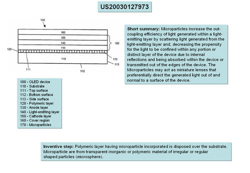
- Microparticles are incorporated in the substrate, which prevents light loss by reflecting light emitted at stray angles.
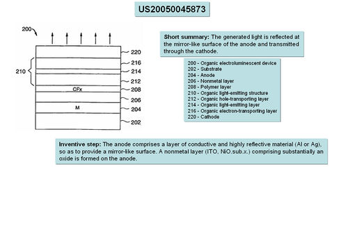
- A highly reflective anode is provided made of Aluminium or Silver, with a mirror like finish, to reflect light.
- A shielding layer is provided below the anode, across its entire surface, thus increasing the surface area from which light can be reflected outside.
- The reflective layer, anode, is made of a highly reflective surface like Aluminium alloy or silver.
Conclusion
The innovation is towards:
- Incorporating micro-particles structure over the substrate that provide a reflective surface.
- Highly reflective materials using metals like Molybdenum etc.
Like this report?
This is only a sample report with brief analysis
Dolcera can provide a comprehensive report customized to your needs
Contact Dolcera
| Samir Raiyani |
|---|
| Email: info@dolcera.com |
| Phone: +1-650-269-7952 |

