Invalidation Search on a patent in the semiconductors space
From DolceraWiki
Contents
- 1 Complementary logic input parallel (CLIP) field effect transistor (FET) logic circuit
- 2 Search report of patent office
- 3 Search strategies
- 4 Non-Patents Analysis
Complementary logic input parallel (CLIP) field effect transistor (FET) logic circuit
Problems and solutions in the prior art
Problem
- Serial connection of the load transistors in conventional CMOS logic gates reduces the toggle rate or switching speed of the gate and also reduces the number of inputs which may be applied to the gate (referred to as "fan-in").
Solutions
- To overcome these problems an "all parallel" CMOS gate design has heretofore been proposed. Here serial load transistors are replaced by a first load which may be an MOS transistor or a resistor, and a second load comprising an MOS transistor having opposite conductivity type from the driver stage transistors.
- A high speed, high density low power dissipation complementary FET logic circuit is disclosed, in which the voltage transfer function of the logic gate's complementary FET inverter output stage is deliberately skewed to dramatically decrease the lift-off interval for the logic gate and thereby dramatically increase the speed of the gate
Problems and solutions for the present invention (CLIP AND & OR logic circuits)
CLIP AND & OR logic circuits according to the invention
Problem - 1
- Rise and delay time was increased
Solution
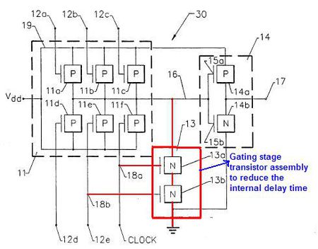
- High speed logic circuit family in which the rise and delay times of the gate are minimized. In other words, the internal delay of the gate in providing a logic output signal which accurately reflects the state of the logic input signals must be minimized.
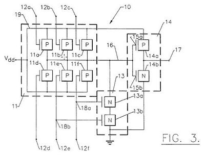
- It has been found, according to the invention that when the geometry of the gating FETs are arranging as described above, the internal delay time of the logic gate is dramatically decreased thereby improving the speed of the gate while still insuring reliable logic switching.
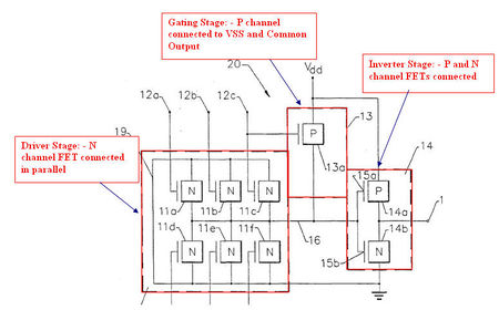
- Geometry of gating FET's: logic gate 10 also includes a gating stage 13 including a pair of gating transistors 13a, 13b serially connected between the common output 16 and the second reference potential (ground). As illustrated in FIG. 3, two gating transistors are used, however any number of gating transistors may be used. Control electrodes 18a and 18b are connected to the control electrodes 12f and 12e of transistors 11f and 11e respectively. Accordingly, gating transistors 13 are turned on when transistors 11e and 11f are turned off. It will be understood by those having skill in the art that control electrodes 18 may be connected to any of control electrodes 12.
- The dimensions of the gating FETs are controlled relative to the dimensions of the driving stage FETs to provide a high speed logic circuit
Problem - 2
- Lower saturation current and corresponding lower carrier mobility of P-channel device compared to N-channel limits the overall speed of the logic gate
Solution
- Provide a high speed complementary all-parallel FET logic family, the performance of which is not limited by the inherently lower saturation current and carrier mobility of P-channel FET devices.
- Speed of the CLIP logic circuits described above is further increased by including germanium in the channels of the P-channel FETs, to thereby increase the carrier mobility in the P-channel FETs. The N-channel FETs are free of germanium so that the carrier mobility of only the P-channel devices is increased. In a preferred embodiment up to 38 atomic percent of the silicon P-channel is germanium, to thereby substantially equalize the carrier mobility of the N-channel FETs and the P-channel FETs. Accordingly, the saturation current limitation of P-channel FETs is reduced and may even be eliminated. It will be understood by those having skill in the art germanium may be included in P-channel FETs of all complementary FET logic circuits to thereby equalize the carrier mobilities in the P and N-channel devices and thereby increase the logic circuit speed.
Problem - 3
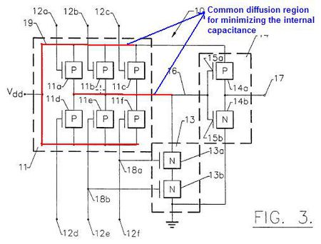
- Internal capacitance of the logic gate also is a major roadblock in increasing its speed. The internal capacitance of the gate also typically limits the number of logic inputs which can be handled by a single gate
Solution
- Provide a high speed complementary all-parallel FET logic family which exhibits low internal capacitance so that large numbers of logic inputs may be handled by a single gate.
- Internal capacitance of the CLIP logic circuits is decreased by using common diffusion regions in the integrated circuit, for pairs of driving stage transistors. The use of the common diffusion region between pairs of FET driving transistors reduces the capacitive loading of the common output by a factor of two thereby further increasing the switching speed of the CLIP logic circuits
- Shared diffusion technique may be used for any all-parallel logic circuit to reduce diffusion capacitance by a factor of two
Other circuits
Clocked CLIP Logic Gates
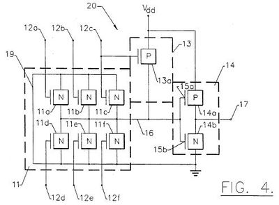
- In the clocked AND gate, the output 17 is high when all of the gates 12a-12e are high and the clock is high.
- In the clocked OR gate, when a clock pulse is applied, clocking FET 21 is turned on and gating FET 13 is turned off. If any one or more of the logic control gates 12a-12f are up then the output of inverter 14 rapidly rises to supply potential Vdd. When the clock pulse drops to ground potential, clocking FET 21 is turned off and gating FET 13 is turned on. When this occurs, the potential of the common output 16 rises rapidly to supply potential Vdd and the output 17 of the inverter 14 rapidly drops to ground potential.
Latching Clocked CLIP Logic Gates
- Latching Clocked CLIP AND gate - Latching FET 23 ensures that the output 17 of complementary inverter 14 remains unchanged during the clock period, regardless of any change in voltage at the inputs 12a-12e.
- Latching Clocked CLIP OR gate -
- The output 17 of complementary inverter 14 is fed back to the gate 24a of the latching FET 23a.
- During the clock pulse interval, if any one of the driving stage transistors 11a-11e is turned on by virtue of its control 12a-12f being at supply potential, the output 17 of the complementary inverter 14 is switched up to supply voltage Vdd. When this condition occurs, FETs 21 and 23 conduct, thereby latching the complementary inverter output 17 up at the supply potential until the end of the clock pulse. When the clock pulse potential drops to ground potential, gating FET 13 turns on and clocking FET 21 turns off, forcing the output of the complementary inverter 14 to rapidly drop to ground potential while simultaneously turning off latching transistor 23
Search report of patent office
- No documents are cited as X or Y attack
Search strategies
Patent search
- Database used - Micropat
| S.No | Scope | Concept | Query | Hits |
| 1 | Claims, Title or Abstract | P or N channel FET’s used to increase the speed, minimize the capacitance, minimize delay time | Query - ((p or n) adj2 (channel or type) NEAR (FET or (field adj1 effect adj1 transistor*))) AND (((increase or step adj1 up or increment or high) NEAR (speed or performance)) OR ((minimize* or reduc* or lower* or (cut adj1 down)) NEAR capacitance) OR ((minimize* or reduc* or lower* or (cut adj1 down)) NEAR delay)) Priority Date (earliest): <19910131 |
134 |
| 2 | Claims, Title or Abstract | Increase the speed of the logic circuits that includes transistors | Query - (increase or step adj1 up or increment or high OR enhanc*) SAME ((logic adj1 (circuit or gate or stage)) AND ((p or n) adj2 (channel or type) NEAR (transistor or *FET*1 or (field adj1 effect adj1 transistor*)))) Priority Date (earliest): <19910131 |
32 |
| 3 | Claims, Title or Abstract | FET’s connected in parallel with the drains connected to Vdd | Query - ((p or n) adj2 (channel or type) NEAR (FET*1 or (field adj1 effect adj1 transistor*))) WITH parallel WITH (Vdd or potential or supply) Priority Date (earliest): <19910131 |
58 |
| 4 | Full patent spec. | FET’s connected in parallel to increase the speed | Query: ((p or n) adj2 (channel or type) NEAR (FET*1 or (field adj1 effect adj1 transistor*))) WITH parallel WITH (Vdd or potential or supply) AND (logic adj1 (circuit or gate)) AND (((increase or step adj1 up or increment or high) NEAR (speed or performance)) OR ((minimize* or reduc* or lower* or (cut adj1 down)) NEAR capacitance) OR ((minimize* or reduc* or lower* or (cut adj1 down)) NEAR delay)) Priority Date (earliest): <19910131 |
33 |
| 5 | Full patent spec. | FET Connection having common output | Query - ((p or n) adj2 (channel or type) NEAR (*FET*1 or (field adj1 effect adj1 transistor*))) SAME (parallel and (Vdd or potential or supply) and (common adj1 output)) Priority Date (earliest): <19910131 |
22 |
| 6 | Full patent spec. | FET’s with channel width, channel lengths and saturation current described | Query: (channel adj1 (width and length)) and (saturation adj1 current) and ((p or n) adj2 (channel or type) NEAR (FET*1 or (field adj1 effect adj1 transistor*))) Priority Date (earliest): <19910131 |
13 |
| 7 | Full patent spec. | FET’s of gating stage connected serially to common output and ground | Query: ((p or n) adj2 (channel or type) NEAR (FET*1 or (field adj1 effect adj1 transistor*))) WITH (((serial or serially) NEAR2 (connected or connection)) and (ground or VSS or potential)) Priority Date (earliest): <19910131 |
98 |
| 8 | Claims | Increasing the speed in the logic circuits | Query - (increase or step adj1 up or increment or high) WITH (logic adj1 (circuit or gate)) AND (transistor or FET*1 or (field effect transisitor*)) and speed Priority Date (earliest): <19910131 |
100 |
| 9 | Full patent spec. | Common diffusion to minimize the internal capacitance | Query: ((common or shared or mutual) WITH diffusion) and ((minimize* or reduc* or lower* or (cut adj1 down)) NEAR capacitance) AND (FET or (field adj1 effect adj1 transistor*) or transistor) Priority Date (earliest): <19910131 | 48 |
| 10 | Full patent spec. | Increasing the carrier mobility in P-channel FET’s by doping germanium | Query - (p adj2 (channel or type) NEAR (transistor or *FET*1 or (field adj1 effect adj1 transistor*))) AND ((increase or step adj1 up or increment or high or enhanc* or equalize) NEAR (carrier NEAR mobilit*)) AND germanium Priority Date (earliest): <19910131 |
12 |
| 11 | Total | 1 OR 2 OR 3 OR 4 OR 5 OR 6 OR 7 OR 8 OR 9 | 542 |
Note: Other databases will also be used to run these queries with the respective operators of the databases. Databases includes SIP, Google patents etc
Non patent search
Technical Articles
- Database used - Google scholar that covers IEEE
- Years - 1985-1990
| S.no | Query | Hits |
| 1 | P N channel FET logic increase OR enhance OR high "speed" | 399 |
| 2 | P channel FET logic speed increase OR enhance OR high "germanium" | 52 |
| 3 | FET logic parallel speed drain increase OR enhance OR high OR Vdd OR potential -patents | 267 |
| 4 | FET logic parallel speed increase OR enhance OR high OR Vdd OR potential "common output" | 30 |
| 5 | P N channel FET logic speed inverter OR complimentary "common output" | 4 |
| 6 | P-channel N-channel FET common diffusion "parallel" | 114 |
| 7 | P-channel N-channel FET germanium increase OR enhance OR high "carrier mobility" | 9 |
| 8 | P-channel N-channel FET germanium increase OR enhance OR high "carrier mobilities" | 3 |
| 9 | P-channel N-channel FET germanium increase OR enhance OR high "saturation current" | 6 |
| 10 | P-channel N-channel FET minimize OR decrease OR reduce "internal capacitance" | 4 |
| 11 | Total | 888 |
Magazine articles
- Found one relevant articles from BYTE magazine.
- Gallium Arsenide Chips - Volume 9, issue 12 (November, 1984)
Non-Patents Analysis
Analysis 1
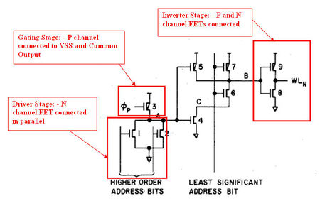
| NAME | CLIP FET | A 15-ns CMOS 64K RAM |
| FIGURE | ||
| TYPE | Patent:- US5247212 | IEEE JOURNAL OF SOLID-STATE CIRCUITS, VOL. SC-21, NO. 5 |
| Title | Complementary logic input parallel (CLIP) logic circuit family | A 15-ns CMOS 64K RAM |
| Assignee | THUNDERBIRD TECH INC (US) | STANLEY E. SCHUSTER, MEMBER, IEEE, BARBARA A. CHAPPELL, MEMBEtt, IEEE, ROBERT L. FRANCH, PAUL F. GREH3R, STEPHEN P. KLEPNER, FANG-SHI J. LA1, MEMBER, IEEE, PETER W. COOK, MEMBER, IEEE, ROBERTA. LIPA, MEMBER, IEEE, REGINALD J. PERRY, WILLIAM F. POKORNY, AND MICHAEL A. ROBERGE |
| IPC | H01L21/8238; H01L27/092; H03K3/356; H03K19/0948; H03K19/096; H01L21/70; H01L27/085; H03K3/00; H03K19/0948; H03K19/096; (IPC1-7): H03K17/04; H03K19/003; H03K19/017; H03K19/094; H03K19/20 | |
| Priority date | 19910131 | |
| Filing date | 19910131 | |
| Publication date | 9/21/1993 | 11/5/1986 |
| Driving stage | P channel FET (CLIP AND gate) / N channel FET (CLIP OR gate) | N channel FET |
| Connection 1 | FET being connected between a common output and a first potential level (Vdd) | FET being connected between a common output and GND |
| Connection 2 | Control electrode of driving stage FET for receiving logic input signals (Multiple) | Control electrode of driving stage FET connected to higher order address lines |
| Gating stage | N channel FET (CLIP AND gate) / P channel FET (CLIP OR gate) | P channel FET |
| Connection 1 | FET being connected between a second potential level (Ground or Vss) and common output. | FET being connected between a second potential level Vss and common output. |
| Connection 2 | Control electrode of gating stage FET is connected to a control electrode of driving stage FET, | Control electrode of gating stage FET is directly/indirectly connected to driving stage which is not shown in figure. It is obvious as the working remains same |
| Complementary FET inverter | Complimentary P & N channel FETs | Complimentary P & N channel FETs |
| Connection 1 | FET’s are serially connected between said first and second potential levels (Vdd and (Vss or grnd)) | FET’s are serially connected between said first and second potential levels (Vdd and (Vss or grnd)) |
| Connection 2 | Inverter input being connected to common output. | Inverter input being connected to common output. |
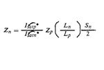
| Zg - channel width of gating transistors, Zd - channel width of driving transistors, I@*satd - saturation current for square channel driving transistor, I@*satg - saturation current for square channel gating transistor, Lg - channel length of gating transistors, Ld - channel length of driving stage transistors, and Sg - number of gating transistors | Since the connections are similar the channel width criteria remains same |
Analysis 2
- Claim 21 - Germanium doped P-channel FET
- The document describes germanium doped P-channel FET for increasing the channel mobility (Page 2630)
Marked document
Conclusion
- The article describes a similar driving stage, gating stage and inverter stage as shown in the above table. Only one extra stage for low order bits is added which is optional can be seen in the figure listed to the right side of above table shown as unmarked stage.
- Hence the article invalidates the inforce patent
