OLED - Organic Light Emitting Diode
Contents
Introduction
The growing number of electronic devices using organic light emitting diode displays shows that after years of promise, the technology is increasingly finding place in many products. But while OLED displays might challenge LCDs as the screens of choice for smaller gadgets, the technology may not become mainstream for notebook PCs or TVs within this decade.
OLED displays use organic compounds that emit light when exposed to an electric current. They are brighter, have better contrast, offer wider viewing angles, use less power, and provide faster response times than liquid crystal displays. OLED screens' thickness is a third of that of LCDs, since they don't need a back-light, and that makes them a good fit for portable electronics devices.
Rationale
- Unlike LCDs, which require backlighting, OLED displays are "emissive" devices, meaning they emit light rather than modulate transmitted or reflected light.
- OLED technology was firstly developed in 1987 at Eastman Kodak Company by Tang and Van Slyke using small-molecule (sm-OLED). In 1990 Richard Friend, Jeremy Burroughes and Donal Bradley discovered electroluminescence capabilities from conjugated polymers so laying down the foundations for a new generation of flat panel displays.
- OLED has the potential to revolutionize the world's $100 billion lighting industry.source
- A light source that could put the traditional light bulb in the shade has been invented by US scientists.source
- OLEDs can provide brighter, crisper displays on electronic devices and use less power than conventional light-emitting diodes (LEDs) or liquid crystal displays (LCDs) used today.source
OLED Components
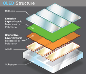
An OLED consists of the following parts:
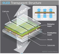
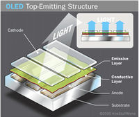
- Substrate (clear plastic, glass, foil) - The substrate supports the OLED.
- Anode (transparent) - The anode removes electrons (adds electron "holes") when a current flows through the device.
- Organic layers - These layers are made of organic molecules or polymers.
- Conducting layer - This layer is made of organic plastic molecules that transport "holes" from the anode. One conducting polymer used in OLEDs is polyaniline.
- Emissive layer - This layer is made of organic plastic molecules (different ones from the conducting layer) that transport electrons from the cathode; this is where light is made. One polymer used in the emissive layer is polyfluorene.
- Cathode (may or may not be transparent depending on the type of OLED) - The cathode injects electrons when a current flows through the device.
Working of OLED'S
- OLEDs emit light in a similar manner to LEDs, through a process called electrophosphorescence.
- The process is as follows:
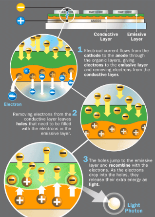
- The battery or power supply of the device containing the OLED applies a voltage across the OLED.
- An electrical current flows from the cathode to the anode through the organic layers (an electrical current is a flow of electrons).
- The cathode gives electrons to the emissive layer of organic molecules.
- The anode removes electrons from the conductive layer of organic molecules. (This is the equivalent to giving electron holes to the conductive layer.)
- At the boundary between the emissive and the conductive layers, electrons find electron holes.
- When an electron finds an electron hole, the electron fills the hole (it falls into an energy level of the atom that's missing an electron).
- When this happens, the electron gives up energy in the form of a photon of light (see How Light Works).
- The OLED emits light.
- The color of the light depends on the type of organic molecule in the emissive layer. Manufacturers place several types of organic films on the same OLED to make color displays.
- The intensity or brightness of the light depends on the amount of electrical current applied: the more current, the brighter the light.
OLED Types
There are several types of OLEDs
- Passive-matrix OLED
- Active-matrix OLED
- Transparent OLED
- Top-emitting OLED
- Bottom-emitting OLED
- Foldable OLED
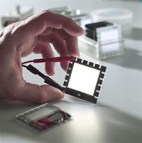
- White OLED
Passive-matrix OLED - PMOLED
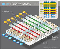
PMOLEDs have strips of cathode, organic layers and strips of anode. The anode strips are arranged perpendicular to the cathode strips. The intersections of the cathode and anode make up the pixels where light is emitted. External circuitry applies current to selected strips of anode and cathode, determining which pixels get turned on and which pixels remain off. Again, the brightness of each pixel is proportional to the amount of applied current.
PMOLEDs are easy to make, but they consume more power than other types of OLED, mainly due to the power needed for the external circuitry. PMOLEDs are most efficient for text and icons and are best suited for small screens (2- to 3-inch diagonal) such as those you find in cell phones, PDAs and MP3 players. Even with the external circuitry, passive-matrix OLEDs consume less battery power than the LCDs that are currently used in these devices.
Active-matrix OLED - AMOLED
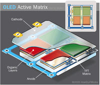
AMOLEDs have full layers of cathode, organic molecules and anode, but the anode layer overlays a thin film transistor (TFT) array that forms a matrix. The TFT array itself is the circuitry that determines which pixels get turned on to form an image.
AMOLEDs consume less power than PMOLEDs because the TFT array requires less power than external circuitry, so they are efficient for large displays. AMOLEDs also have faster refresh rates suitable for video. The best uses for AMOLEDs are computer monitors, large screen TVs and electronic signs or billboards.
Transparent OLED
Transparent OLEDs have only transparent components (substrate, cathode and anode) and, when turned off, are up to 85 percent as transparent as their substrate. When a transparent OLED display is turned on, it allows light to pass in both directions. A transparent OLED display can be either active- or passive-matrix. This technology can be used for heads-up displays.
Top-emitting OLED
Top-emitting OLEDs have a substrate that is either opaque or reflective. They are best suited to active-matrix design. Manufacturers may use top-emitting OLED displays in smart cards.
Foldable OLED
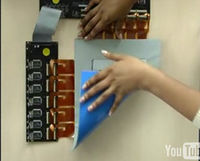
Foldable OLEDs have substrates made of very flexible metallic foils or plastics. Foldable OLEDs are very lightweight and durable. Their use in devices such as cell phones and PDAs can reduce breakage, a major cause for return or repair. Potentially, foldable OLED displays can be sewn into fabrics for "smart" clothing, such as outdoor survival clothing with an integrated computer chip, cell phone, GPS receiver and OLED display sewn into it.
White OLED
A white organic LED (OLED) incorporating a blue phosphorescent dye and a down-conversion phosphor has achieved a luminous efficacy of 25 lm/W. This high-efficacy device was enabled by lowering the device operating voltage, increasing the outcoupling efficiency, and incorporating highly efficient phosphorescent emitters.
OLED Advantages and Disadvantages
OLEDs offer many advantages over both LCDs and LEDs:
- The plastic, organic layers of an OLED are thinner, lighter and more flexible than the crystalline layers in an LED or LCD.
- Because the light-emitting layers of an OLED are lighter, the substrate of an OLED can be flexible instead of rigid. OLED substrates can be plastic rather than the glass used for LEDs and LCDs.
- OLEDs are brighter than LEDs. Because the organic layers of an OLED are much thinner than the corresponding inorganic crystal layers of an LED, the conductive and emissive layers of an OLED can be multi-layered. Also, LEDs and LCDs require glass for support, and glass absorbs some light. OLEDs do not require glass.
- OLEDs do not require backlighting like LCDs. LCDs work by selectively blocking areas of the backlight to make the images that you see, while OLEDs generate light themselves. Because OLEDs do not require backlighting, they consume much less power than LCDs (most of the LCD power goes to the backlighting). This is especially important for battery-operated devices such as cell phones.
- OLEDs are easier to produce and can be made to larger sizes. Because OLEDs are essentially plastics, they can be made into large, thin sheets. It is much more difficult to grow and lay down so many liquid crystals.
- OLEDs have large fields of view, about 170 degrees. Because LCDs work by blocking light, they have an inherent viewing obstacle from certain angles. OLEDs produce their own light, so they have a much wider viewing range.
OLED seems to be the perfect technology for all types of displays, but it also has some problems:
- Lifetime - While red and green OLED films have longer lifetimes (46,000 to 230,000 hours), blue organics currently have much shorter lifetimes (up to around 14,000 hours.
- Water - Water can easily damage OLEDs.
Control Patents
| S.No | Patent/Publication No. | Date of Publication | Assignee / Applicant | Title |
| 1 | US7791271B2 | 09/07/2010 | Global OLED Technology LLC | Top-emitting OLED device with light-scattering layer and color-conversion |
| 2 | US7781961B2 | 08/24/2010 | Novaled AG | Top emitting, electroluminescent component with frequency conversion centres |
| 3 | US7002293B2 | 02/21/2006 | Eastman Kodak Company | Organic light emitting diode with improved light emission through the cathode |
| 4 | US6770502B2 | 08/03/2004 | Eastman Kodak Company | Method of manufacturing a top-emitting OLED display device with desiccant structures |
| 5 | US20080169757A1 | 07/17/2008 | TPO Displays Corp. | Top-emitting organic electroluminescent display |
| 6 | US20060043373A1 | 03/02/2006 | Industrial Technology Research Institute | Method for manufacturing a pixel array of top emitting OLED |
| 7 | US20050236629A1 | 10/27/2005 | None | Top emission organic light emitting diode display using auxiliary electrode to prevent voltage drop of upper electrode and method of fabricating the same |
| 8 | EP1489671A2 | 12/22/2004 | Global OLED Technology LLC | Method of making a top-emitting oled device having improved power distribution |
| 9 | EP1029336A1 | 08/23/2000 | FED CORPORATION | TOP EMITTING OLED WITH REFRACTORY METAL COMPOUNDS AS BOTTOM CATHODE |
| 10 | WO2001057904A1 | 08/09/2001 | eMAGIN CORPORATION | LOW ABSORPTION SPUTTER PROTECTION LAYER FOR OLED STRUCTURE |
Concept Table
| Top emission | Organic Light Emitting Diode |
| Top emitting | OLED |
| Top emissive | polymer LED |
| light emitting polymer diode | |
| organic LED | |
| organic electroluminescent diode | |
| FOLED | |
| SM-OLED | |
| small molecule OLED | |
| AMOLED | |
| PMOLED |
Classifications
IPC/ ECLA Classes
| IPC/ ECLA Class | Definition |
| H01L27/28 | Devices consisting of a plurality of semiconductor or other solid state components formed in or on a common substrate/ including components using organic materials as the active part, or using a combination of organic materials with other materials as the active part |
| H01L27/32 | Devices consisting of a plurality of semiconductor or other solid state components formed in or on a common substrate/ including components using organic materials as the active part, or using a combination of organic materials with other materials as the active part/ with components specially adapted for light emission, e.g. flat-panel displays using organic light-emitting diodes (OLED) |
| H01L51/50 | Solid state devices using organic materials as the active part, or using a combination of organic materials with other materials as the active part; Processes or apparatus specially adapted for the manufacture or treatment of such devices, or of parts thereof / specially adapted for light emission, e.g. organic light emitting diodes (OLED) or polymer light emitting devices (PLED); |
| H01L51/52 | Solid state devices using organic materials as the active part, or using a combination of organic materials with other materials as the active part; Processes or apparatus specially adapted for the manufacture or treatment of such devices, or of parts thereof / specially adapted for light emission, e.g. organic light emitting diodes (OLED) or polymer light emitting devices (PLED);/ details of devices |
| H01L51/56 | Solid state devices using organic materials as the active part, or using a combination of organic materials with other materials as the active part; Processes or apparatus specially adapted for the manufacture or treatment of such devices, or of parts thereof / specially adapted for light emission, e.g. organic light emitting diodes (OLED) or polymer light emitting devices (PLED);/ Processes or apparatus specially adapted for the manufacture or treatment of such devices or of parts thereof |
| H05B33/08P | Electroluminescent light sources / Details/ Circuit arrangements not adapted to a particular application/ for light emitting diodes (LEDs) comprising organic materials, e.g. polymer LEDs (PLEDs) or OLEDs] |
US Classes
| US Class | Definition |
| 257/040 | Active solid-state devices (e.g., transistors, solid-state diodes)/ Organic semiconductor material |
| 257/E51.018 | Organic solid state devices, processes or apparatus peculiar to manufacture or treatment of such devices or of parts thereof/ Structural detail of device/ Light-emitting organic solid-state device with potential or surface barrier |
| 257/E51.019 | Organic solid state devices, processes or apparatus peculiar to manufacture or treatment of such devices or of parts thereof/ Structural detail of device/ Light-emitting organic solid-state device with potential or surface barrier/ Electrode |
| 257/E51.020 | Organic solid state devices, processes or apparatus peculiar to manufacture or treatment of such devices or of parts thereof/ Structural detail of device/ Light-emitting organic solid-state device with potential or surface barrier/ Electrode/ Encapsulation |
| 257/E51.021 | Organic solid state devices, processes or apparatus peculiar to manufacture or treatment of such devices or of parts thereof/ Structural detail of device/ Light-emitting organic solid-state device with potential or surface barrier/ Electrode/ Arrangements for extracting light from device (e.g., Bragg reflector pair) |
| 257/E51.022 | Organic solid state devices, processes or apparatus peculiar to manufacture or treatment of such devices or of parts thereof/ Structural detail of device/ Light-emitting organic solid-state device with potential or surface barrier/ Multicolor organic light-emitting device (OLED) |
| 313/504 | Electric lamp and discharge devices/ with luminescent solid or liquid material / Solid-state type / With particular phosphor or electrode material / Organic phosphor |
Taxonomy
Micropatent Search Strategy
- A search is carried out in Micropatent using a combination of keywords and classifications
- Databases covered: US Granted, US Applications, EP-A, EP-B, WO, JP(bibliographic data), DE-C,B, DE-A, DE-T, DE-U, GB-A, FR-A
| |
|
|
|
|
| |
|
|
Any Classification | H01L005150* OR H01L005152* OR H01L005156 OR H05B003308P OR 257E51.022 |
| |
|
|
Any Classification | 313504 OR 257040 OR 257E51.018 OR 257E51.019 OR 257E51.020 OR 257E51.021 OR H01L002728 OR H01L002732 |
| |
|
|
Claims, Title or Abstract | ((Top emitting) or (TOLED) or (TEOLED) or (TE-OLED) or (Top adj2 emitting) or (Top adj2 emissive) or (Top adj2 emission)) adj ((Light adj emitting adj polymer) OR (Organic adj electro-luminescence adj diode) OR (organic adj electroluminescent adj diode) OR (Ploymer adj light adj emitting adj diode) OR (Organic adj light adj emitting adj device) OR (Self-luminous adj diode) OR (OLED) OR (Organic LED arrays) OR (Organic adj light adj emitting adj diode) OR (Organic adj light adj emission adj diode) OR (Polymer adj light adj emission adj device) OR (organic adj electroluminescent device) OR (OEL) OR (OLEDs)) |
| |
|
|
Claims, Title or Abstract | (((organic or (small adj molecule*1) or polymer*1) adj (lightemitting or (light adj (emitting or emission)) or electroluminescen*2 or (electro adj luminescen*2))) near3 diode*1) Or OLED*2 or SMLED*2 or PLED*2 or (light adj (emitting or emission) adj polymer*1) or ((organic or (small adj molecule*1) or polymer*1) near3 LED*2) |
| |
|
|
Claims, Title or Abstract | (((((organic or (small adj molecule*1) or polymer*1) adj (lightemitting or (light adj (emitting or emission)) or electroluminescen*2 or (electro adj luminescen*2))) near3 diode*1) Or OLED*2 or SMLED*2 or PLED*2 or (light adj (emitting or emission) adj polymer*1) or ((organic or (small adj molecule*1) or polymer*1) near3 LED*2)) AND ((top adj3 (emissi*2 or emitting)))) or (TE adj OLED*2) |
| |
|
|
Combined query | 1 and 3 |
| |
|
|
Claims, Title or Abstract | ((lightemitting or (light adj (emitting or emission)) or electroluminescen*2 or (electro adj luminescen*2)) near3 diode*1) or LED*2 or OLED*2 or SMLED*2 or PLED*2 |
| |
|
|
Combined query | 2 and 7 and 3 |
| |
|
|
Full patent spec. | (((((organic or (small adj molecule*1) or polymer*1) adj (lightemitting or (light adj (emitting or emission)) or electroluminescen*2 or (electro adj luminescen*2))) near3 diode*1) Or OLED*2 or SMLED*2 or PLED*2 or (light adj (emitting or emission) adj polymer*1) or ((organic or (small adj molecule*1) or polymer*1) near3 LED*2)) near3 ((top adj3 (emissi*2 or emitting)))) or (TE adj OLED*2) |
| |
|
|
Full patent spec. | ((top adj3 (emissi*2 or emitting)) or (Top near2 emittierende*1)) near3 ((organische near2 (LED*1 or Leuchtdiode*1)) or (Licht adj emittierende adj Polymer*1) or OLED*1) |
| |
|
|
Full patent spec. | ((top adj3 (émissive or émettant)) or (démission adj top) or (top adj3 (emissi*2 or emitting))) near3 ((diode*1 near3 électroluminescente near3 organique*1) or ((Polymère*1 or organiques) adj2 LED*1) or (polymère*1 near3 émettant near3 lumière) or OLED*1) |
| |
|
Combined query | 5 or 6 or 8 or 9 or 10 or 11 | |
| |
|
|
Patent/Publication No. | WO2001057904A1 OR EP1029336A1 OR EP1489671A2 OR US20050236629A1 OR US20060043373A1 OR US20080169757A1 OR US6770502B2 OR US7002293B2 OR US7781961B2 OR US7791271B2 |
| |
|
Combined query | 12 AND 13 |
Landscape Analysis Of Top-Emmission OLED
IP Landscape
- We have chosen the top emission OLED's as the area of focus.
- The top emission OLED's have been facing challenges to achieve optimimum efficiencies in terms of light reflection. Also, it's been a challenge to increase the life time of the top emission OLED's. Lots of initiative is seen in this direction, and below is a snapshot of research work done by organizations worldwide to achieve higher efficiency levels through better design.
Like this report?
This is only a sample report with brief analysis
Dolcera can provide a comprehensive report customized to your needs
Competitor Landscape
Competitor Mapping
| # | Assignee Name | 2001 | 2002 | 2003 | 2004 | 2005 | 2006 | 2007 | Total |
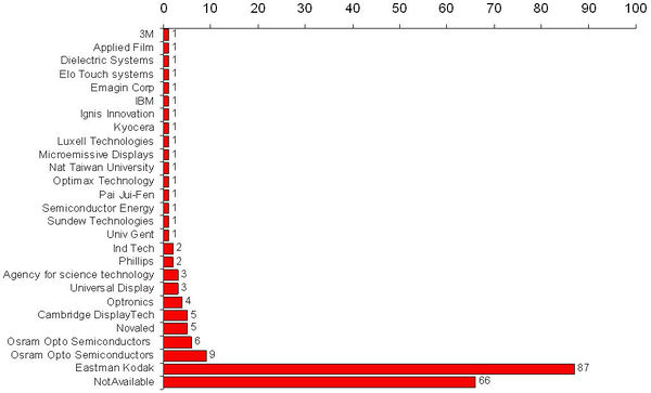
| 1 | Eastman Kodak | 1 | 3 | 23 | 24 | 24 | 12 | 87 | |
| 2 | Not Available | 3 | 10 | 9 | 20 | 18 | 6 | 66 | |
| 3 | Osram Opto Semiconductors | 2 | 1 | 4 | 2 | 9 | |||
| 4 | Osram Opto Semiconductors | 1 | 2 | 3 | 6 | ||||
| 5 | Cambridge DisplayTech | 1 | 4 | 5 | |||||
| 6 | Novaled | 1 | 2 | 2 | 5 | ||||
| 7 | Optronics | 4 | 4 | ||||||
| 8 | Agency for science technology | 2 | 1 | 3 | |||||
| 9 | Universal Display | 1 | 2 | 3 | |||||
| 10 | Ind Tech | 2 | 2 | ||||||
| 11 | Phillips | 1 | 1 | 2 | |||||
| 12 | 3M | 1 | 1 | ||||||
| 13 | Applied Film | 1 | 1 | ||||||
| 14 | Dielectric Systems | 1 | 1 | ||||||
| 15 | Elo Touch systems | 1 | 1 | ||||||
| 16 | Emagin Corp | 1 | 1 | ||||||
| 17 | IBM | 1 | 1 | ||||||
| 18 | Ignis Innovation | 1 | 1 | ||||||
| 19 | Kyocera | 1 | 1 | ||||||
| 20 | Luxell Technologies | 1 | 1 | ||||||
| 21 | Microemissive Displays | 1 | 1 | ||||||
| 22 | Nat Taiwan University | 1 | 1 | ||||||
| 23 | Optimax Technology | 1 | 1 | ||||||
| 24 | Pai Jui-Fen | 1 | 1 | ||||||
| 25 | Semiconductor Energy | 1 | 1 | ||||||
| 26 | Sundew Technologies | 1 | 1 | ||||||
| 27 | Univ Gent | 1 | 1 | ||||||
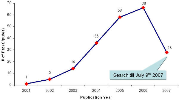
| 28 | Total | 1 | 5 | 14 | 36 | 58 | 66 | 28 | 208 |
Key Inventors
Key Inventor Mapping
| S.No | Top 10 Assignees of Last 5 Years | 2001 | 2002 | 2003 | 2004 | 2005 | 2006 | 2007 | Total |
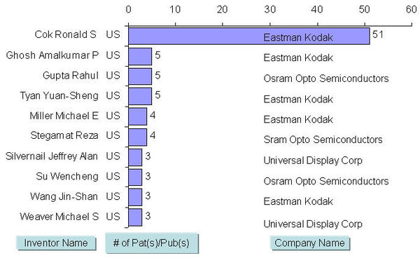
| 1 | Cok Ronald S US | 2 | 12 | 13 | 13 | 11 | 51 | ||
| 2 | Ghosh Amalkumar P US | 1 | 2 | 2 | 5 | ||||
| 3 | Gupta Rahul US | 5 | 5 | ||||||
| 4 | Tyan Yuan-Sheng US | 1 | 3 | 1 | 5 | ||||
| 5 | Miller Michael E US | 1 | 1 | 2 | 4 | ||||
| 6 | Stegamat Reza US | 2 | 1 | 1 | 4 | ||||
| 7 | Silvernail Jeffrey Alan US | 2 | 1 | 3 | |||||
| 8 | Su Wencheng US | 1 | 2 | 3 | |||||
| 9 | Wang Jin-Shan US | 3 | 3 | ||||||
| 10 | Weaver Michael S US | 1 | 2 | 3 | |||||
| Total | 5 | 19 | 26 | 23 | 13 | 86 |
Technology Mapping
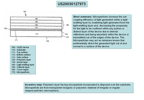
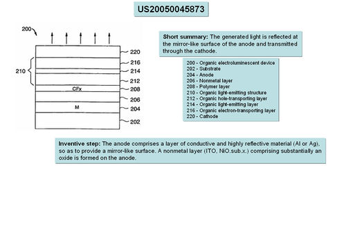
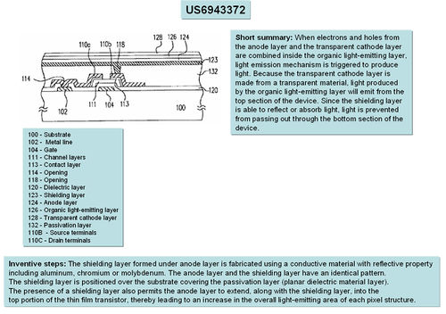
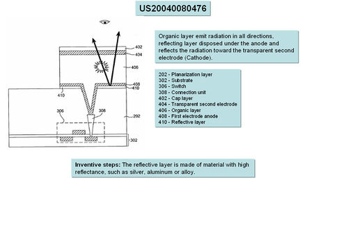
- In OLED devices not all internally generated light is coupled out of the device (only 20%-50%), which reduces the device efficiency and lifetime.
- Modification in structures are applied to improve outcouple efficiency in order to enhance the efficiency and lifetime of top emission OLEDs.
- Below is a snapshot of how various organizations are using different design structures, using the same principle of internal reflection, to achieve higher out-coupling efficiencies.
Comparison of out coupling of waveguiding light in top-emission polyLED stack
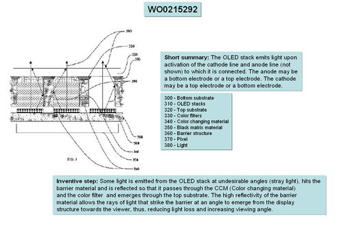
- Some light is reflected out of the OLED at stray angles in typical cases. By using a barrier material (form of microparticles) in the cathode layer, this light at stray angles hits the barrier material, and some of it is reflected back and guided out at the right angles, reducing light loss.
- Microparticles are incorporated in the substrate, which prevents light loss by reflecting light emitted at stray angles.
- A highly reflective anode is provided made of Aluminium or Silver, with a mirror like finish, to reflect light.
- A shielding layer is provided below the anode, across its entire surface, thus increasing the surface area from which light can be reflected outside.
- The reflective layer, anode, is made of a highly reflective surface like Aluminium alloy or silver.
Conclusion
The innovation is towards:
- Incorporating micro-particles structure over the substrate that provide a reflective surface.
- Highly reflective materials using metals like Molybdenum etc.
Like this report?
This is only a sample report with brief analysis
Dolcera can provide a comprehensive report customized to your needs
Contact Dolcera
| Samir Raiyani |
|---|
| Email: info@dolcera.com |
| Phone: +1-650-269-7952 |
