Difference between pages "Transactional memory in hardware" and "Carbon Nanotubes (CNT)"
Manikandan (Talk | contribs) (→Patent dashboard) |
Manikandan (Talk | contribs) (→Contact Dolcera) |
||
| Line 1: | Line 1: | ||
| − | == | + | == Introduction == |
| − | + | ||
| − | + | ||
| − | + | ||
| − | + | ||
| − | + | ||
| − | + | ||
| − | |||
| − | === | + | === Nanotechnology === |
| − | + | Nanotechnology refers broadly to a field of applied science and technology whose unifying theme is the control of matter on the atomic and molecular scale, normally 1 to 100 nanometers, and the fabrication of devices with critical dimensions that lie within that size range. | |
| − | + | ||
| − | + | ||
| − | + | ||
| + | === Run of Nanotechnology === | ||
| + | * '''December 29, 1959''': The first thought of Nanotechnology was given by Richard Feynman in "[http://www.zyvex.com/nanotech/feynman.html There's Plenty of Room at the Bottom]" at an American Physical Society meeting at Caltech. | ||
| + | * '''September, 1981''': First technical paper published on molecular nanotechnology. The same year scanning tunneling microscope (STM) invented. | ||
| + | * '''1982-1990''':Books and prizes on nanotechnology. Atomic force microscope invented in 1986. | ||
| + | * '''1991''': Carbon Nanotubes (CNT's) discovered. | ||
| + | * '''1997''': First company on nanotechnology founded, it's name is [http://www.zyvex.com/ Zyvex]. | ||
| + | * '''1998-2007''': Research, investment, conferences and meetings on nanotechnology. | ||
| − | === | + | === Applications of Nanotechnology === |
| − | + | It has or will have applications in almost all areas we can think of. | |
| − | ==== | + | {|border="2" cellspacing="0" cellpadding="4" width="100%" |
| − | *[http:// | + | |- |
| − | + | !Environment and Energy || Medical and Health || Electronics and Computers || Space, Aircraft and Transportation || Materials and Manufacturing | |
| + | |- | ||
| + | | valign = "top" | | ||
| + | * Clean Technology | ||
| + | * Reducing Global Warming | ||
| + | * Eco-friendly and Efficient Energy | ||
| + | * Eco-friendly Coatings | ||
| + | * Lotus-effect Surfaces | ||
| + | * Self-cleaning Glass | ||
| + | * Environmental Monitoring | ||
| + | * Remediation of Soil | ||
| + | * Remediation and Treatment of Water | ||
| + | | valign = "top" | | ||
| + | * Lab-on-a-chip: The Analytical Revolution | ||
| + | * Nanoparticles and Drug Delivery | ||
| + | * Nanoparticles and Gene Therapy | ||
| + | * Textured Surfaces for Tissue Regeneration | ||
| + | * Nanorobot Therapeutics | ||
| + | | valign = "top" | | ||
| + | * Desktop Manufacturing | ||
| + | * Electronic Paper | ||
| + | * Nanoelectronics and Computing | ||
| + | * Assemblers and Self-replicators | ||
| + | * Molecular Electronics | ||
| + | | valign = "top" | | ||
| + | * Space and Aeronautics | ||
| + | * Automobiles | ||
| + | * Transportation Infrastructure | ||
| + | | valign = "top" | | ||
| + | * New and Nanostructured Materials | ||
| + | * Nano-engineered Advanced Materials | ||
| + | * NanoGold: Carbon Nanotubes | ||
| + | * Potential Industrial Applications | ||
| + | |- | ||
| + | |} | ||
| + | ([http://www.nipne.ro/rjp/2004_49_9-10/0767_0776.pdf Source link]) | ||
| + | * '''Aerospace''' | ||
| + | ::* [http://www.pbs.org/wgbh/nova/sciencenow/3401/02.html Space Elevators] | ||
| + | ::* [http://science.nasa.gov/headlines/y2002/16sep_rightstuff.htm Spaceship] | ||
| + | ::* [http://www.andybrain.com/extras/solar-sail.htm Solar Sails] | ||
| + | ::* [http://www.niac.usra.edu/files/library/meetings/annual/oct04/914Mavroidis.pdf Biorobots] | ||
| + | * '''Medicine''' | ||
| + | ::* Identifying location of cancer cells. [http://www.physorg.com/news2850.html] | ||
| + | ::* Delivering chemotherapy drugs directly to cancer cells.[http://www.rsc.org/chemistryworld/News/2006/April/11040601.asp] | ||
| + | ::* Nanoshells that concentrate the heat from infrared light to destroy cancer cells with minimal damage to surrounding healthy cells. [http://www.sciencentral.com/articles/view.php3?language=english&type=24119&article_id=218392390&cat=3_all] | ||
| + | ::* Nanotubes used in broken bones to provide a structure for new bone material to grow.[http://www.physorg.com/news5003.html] | ||
| + | ::* Nanoparticles that can attach to cells infected with various diseases and allow a lab to identify, in a blood sample, the particular disease.[http://www.nanotech-now.com/news.cgi?story_id=16228] | ||
| + | * '''Food Storage''' | ||
| + | ::* [http://www.nanocor.com/nanocomposites.asp Clay nanocomposites] are being used to provide an impermeable barrier to gasses such as oxygen or carbon dioxide in lightweight bottles, cartons and packaging films. | ||
| + | ::* Food storage bins are being produced with silver nanoparticles embedded in the plastic. The silver nanoparticles kill bacteria from any food that was previously stored in the bins, minimizing health risks from harmful bacteria.[http://www.azonano.com/details.asp?ArticleID=1695] | ||
| + | ::* It is possible to use nanosensors in plastic packaging to detect gases given off by food when it spoils. The packaging itself changes color to alert you to food gone bad. | ||
| + | * '''Agriculture''' | ||
| + | ::* Food will be more tastier and healthier using nanaotechnology.[http://nsrg.neu.edu/resources/regulatory_capacity/documents/NanoAgFood.pdf] | ||
| + | ::* Research is also being conducted to develop nanocapsules containing nutrients that would be released when nanosensors detect a vitamin deficiency in your body. | ||
| + | ::* Researchers are also working on pesticides encapsulated in nanoparticles; that only release pesticide within an insect’s stomach, minimizing the contamination of plants themselves. | ||
| + | ::* Another development being persued is a network of nanosensors and dispensers used throughout a food crop. The sensors recognize when a plant needs nutrients or water, before there is any sign that the plant is deficient. The dispensers then release fertilizer, nutrients, or water as needed, optimizing the growth of each plant in the field one by one. | ||
| + | * '''Chemistry''' | ||
| + | ::* Nanoparticles can be used as catalyst for chemical reactions. | ||
| + | ::* Nanotechnology can enable sensors to detect very small amounts of chemical vapors.[http://people.nas.nasa.gov/~cwei/Publication/cnt_sensor.pdf] | ||
| + | ::* ZnO nanowires may lead to better chemical sensors, high-speed electronics.[http://www.physorg.com/news77303473.html] | ||
| + | ::* Palladium nanoparticle hydrogen sensor.[http://nano-proprietary.com/PDFs/Palladium%20Nanoparticle%20Hydrogen%20SensorMNPS.pdf] | ||
| + | * '''Semiconductor devices''' | ||
| + | ::* [http://en.wikipedia.org/wiki/Nanoelectromechanical_systems NEMS] | ||
| + | ::* [http://www.technologyreview.com/Nanotech/18591/ OLED] | ||
| + | ::* [http://www.zurich.ibm.com/st/storage/concept.html Memory chips] | ||
| + | ::* [http://www.motorola.com/content.jsp?globalObjectId=8206 Nanoemmissive display panel] | ||
| + | ::* [http://www.intel.com/technology/architecture-silicon/45nm-core2/index.htm 45 nm wide transistor gates] | ||
| + | ::* [http://www.voyle.net/Nano%20Electronics/Nano%20Electronics-2004-0040.htm Magnetoresistive Random Access Memory (MRAM)] | ||
| + | ::* [http://www.hpl.hp.com/research/about/nanoelectronics.html Nanoscale integrated circuits] | ||
| + | * '''Optics''' | ||
| + | ::* The first sunglasses using protective and antireflective ultrathin polymer coatings are on the market. | ||
| + | ::* Nanotechnology also offers scratch resistant surface coatings based on nanocomposites. | ||
| + | ::* Nano-optics could allow for an increase in precision of pupil repair and other types of laser eye surgery. | ||
| + | * '''Textile''' | ||
| + | ::* The use of engineered nanofibers already makes clothes water- and stain-repellent or wrinkle-free. | ||
| + | ::* Textiles with a nanotechnological finish can be washed less frequently and at lower temperatures. | ||
| + | ::* Nanotechnology has been used to integrate tiny carbon particles membrane and guarantee full-surface protection from electrostatic charges for the wearer. | ||
| + | * '''Consumer products''' | ||
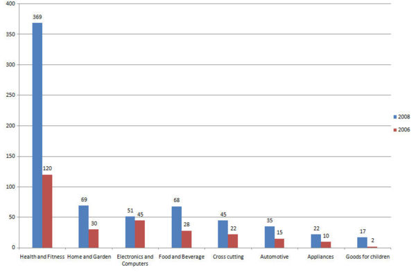
| + | ::* Nanotechnology is now entered in almost all consumer products,for details see [http://www.nanotechproject.org/inventories/consumer/browse/] | ||
| − | + | [[Image:report9.jpg|center|600 px|thumb|Number of products launched products launched vs categories]] | |
| − | + | ||
| − | + | ||
| − | + | ||
| − | + | [http://www.nanotechproject.org/inventories/consumer/analysis_draft/ Source link] | |
| − | + | ||
| − | + | ||
| − | == | + | == Carbon Nanotubes == |
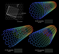
| − | + | [[Image:carbonnanotubes.png|Right|200 px|thumb|3D model of three types of single-walled carbon nanotubes]] | |
| − | + | ||
| − | + | Carbon Nanotubes (CNT's) are cylindrical shaped allotrope of carbon with | |
| + | length to diameter ratio exceeding 1,000,000. | ||
| − | + | Such cylindrical carbon molecules have novel properties that make | |
| − | + | them potentially useful in many applications in nanotechnology, | |
| − | + | electronics, optics and other fields of materials science. They | |
| + | exhibit extraordinary strength and unique electrical properties, | ||
| + | and are efficient conductors of heat. | ||
| − | === | + | === Types === |
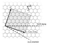
| − | + | [[Image:swcnt.jpg|right|200 px|thumb|Vectors representing orientation of three types of Single-walled CNT's]] | |
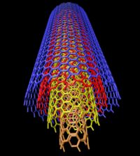
| − | *''' | + | [[Image:dwcnt.jpg|right|200 px|thumb|A Double-walled CNT formed by multiple Single-walled CNTs]] |
| + | # '''[http://www.pa.msu.edu/cmp/csc/ntproperties/equilibriumstructure.html Single-walled CNT's]''': This type of nanotube can be formed by rolling Graphene sheet. Graphene is a single planar sheet of sp²-bonded carbon atoms that are densely packed in a honeycomb crystal lattice. Types of Single-walled CNT's: | ||
| + | #* Zig-zag(n,0) | ||
| + | #* Armchair(n,n) | ||
| + | #* Chiral(2n,n) | ||
| + | # '''[http://www.nanotech-now.com/nanotube-buckyball-sites.htm Multi-walled]''': Multi-walled nanotubes(MWNT) consist of multiple layers of graphite rolled in on themselves to form a tube shape. | ||
| + | # '''[http://en.wikipedia.org/wiki/Fullerene Fullerite]''': Fullerites are the solid-state manifestation of fullerenes and related compounds and materials. Being highly incompressible nanotube forms, polymerized single-walled nanotubes (P-SWNT) are a class of fullerites and are comparable to diamond in terms of hardness. | ||
| + | # '''[http://en.wikipedia.org/wiki/Torus Torus]''': A nanotorus is a theoretically described carbon nanotube bent into a torus (doughnut shape). | ||
| + | # '''[http://en.wikipedia.org/wiki/Carbon_nanobud Nanobud]''': The material fullerene-like "buds" are covalently bonded to the outer sidewalls of the underlying carbon nanotube. This hybrid material has useful properties of both fullerenes and carbon nanotubes. | ||
| − | ===== | + | === Properties === |
| − | + | ::* '''Physical Properties''' | |
| − | *''' | + | {|border="2" cellspacing="0" cellpadding="4" width="65%" |
| + | |align = "center" bgcolor = "#D9D9D9"|'''Material''' | ||
| + | |align = "center" bgcolor = "#D9D9D9"|'''Young<nowiki>’</nowiki>s modulus''' (GPa) | ||
| + | |align = "center" bgcolor = "#D9D9D9"|'''Tensile Strength''' (GPa) | ||
| + | |align = "center" bgcolor = "#D9D9D9"|'''Density''' (g/cm3) | ||
| + | |- | ||
| + | |align = "center"|Single wall nanotube | ||
| + | |align = "center"|1054 | ||
| + | |align = "center"|150 | ||
| + | |align = "center"|N/A | ||
| + | |- | ||
| + | |align = "center"|Multi wall nanotube | ||
| + | |align = "center"|1200 | ||
| + | |align = "center"|150 | ||
| + | |align = "center"|2.6 | ||
| + | |- | ||
| + | |align = "center"|Steel | ||
| + | |align = "center"|208 | ||
| + | |align = "center"|0.4 | ||
| + | |align = "center"|7.8 | ||
| + | |- | ||
| + | |align = "center"|Epoxy | ||
| + | |align = "center"|3.5 | ||
| + | |align = "center"|0.005 | ||
| + | |align = "center"|1.25 | ||
| + | |- | ||
| + | |align = "center"|Wood | ||
| + | |align = "center"|16 | ||
| + | |align = "center"|0.008 | ||
| + | |align = "center"|0.6 | ||
| + | |- | ||
| + | |} | ||
| + | [http://www.applied-nanotech.com/cntproperties.htm Source link] | ||
| + | ::* '''Electrical Properties''': Because of the symmetry and unique electronic structure of graphene, the structure of a nanotube strongly affects its electrical properties. For a given (n,m) nanotube, if n − m is a multiple of 3, then the nanotube is metallic, otherwise the nanotube is a semiconductor. Thus all armchair (n=m) nanotubes are metallic, and nanotubes (5,0), (6,4), (9,1), etc. are semiconducting. In theory, metallic nanotubes can have an electrical current density more than 1,000 times greater than metals such as silver and copper. | ||
| − | === | + | === Method of fabrication === |
| − | * | + | ::* '''[http://nanotube.msu.edu/synthesis/ca.html Arc discharge]''': It is the simplest and most commonly used method of producing Carbon nanotubes. This method creates CNTs through arc-vaporization of two carbon rods placed end to end, separated by approximately 1mm, in an enclosure that is usually filled with inert gas (helium, argon) at low pressure (between 50 and 700 mbar). |
| − | * | + | ::* '''[http://www.azonano.com/Details.asp?ArticleID=1561 Laser ablation]''': In 1996, a dual-pulsed laser vaporization technique was developed, which produced SWNTs in gram quantities and yields of >70wt% purity. Samples were prepared by laser vaporization of graphite rods with a 50:50 catalyst mixture of Co and Ni (particle size ~1um) at 1200oC in flowing argon, followed by heat treatment in a vacuum at 1000oC to remove the C60 and other fullerenes. |
| − | * | + | ::* '''[http://en.wikipedia.org/wiki/Chemical_vapor_deposition Chemical vapor deposition (CVD)]''':Large amounts of CNTs can be formed by catalytic CVD of acetylene over Co and Fe catalysts supported on silica or zeolite. |
| − | + | ||
| − | + | ||
| − | == | + | == Application of Carbon nanotubes == |
| − | * | + | ::* '''Polymer Composites''': The first realized major commercial application of MWNTs is their use as electrically conducting components in polymer composites.Depending on the polymer matrix, conductivities of 0.01 to 0.1 S/cm can be obtained for 5% loading; much lower conductivity levels suffice for dissipating electrostatic charge. The low loading levels and the nanofiber morphology of the MWNTs allow electronic conductivity to be achieved while avoiding or minimizing degradation of other performance aspects, such as mechanical properties and the low melt flow viscosity needed for thin-wall molding applications. |
| − | * | + | ::* '''Electrochemical devices''': Because of the high electrochemically accessible surface area of porous nanotube arrays, combined with their high electronic conductivity and useful mechanical properties, these materials are attractive as electrodes for devices that use electrochemical double-layer charge injection. |
| + | ::* '''Hydrogen storage''': Nanotubes have been long heralded as potentially useful for hydrogen storage (for example, for fuel cells that power electric vehicles or laptop computers). | ||
| + | ::* '''Field emission devices''': Industrial and academic research activity on electronic devices has focused principally on using SWNTs and MWNTs as field emission electron sources for flat panel displays, lamps, gas discharge tubes providing surge protection, and x-ray and microwave generators. | ||
| + | ::* '''Nanometer-sized electronic devices''': | ||
| + | ::* '''Sensors and probes''': Possible chemical sensor applications of nonmetallic nanotubes are interesting, because nanotube electronic transport and thermopower (voltages between junctions caused by interjunction temperature differences) are very sensitive to substances that affect the amount of injected charge.The main advantages are the minute size of the nanotube sensing element and the correspondingly small amount of material required for a response. | ||
| − | + | [http://www.eikos.com/articles/carbnano_routetoapp.pdf Source link] | |
| − | + | ||
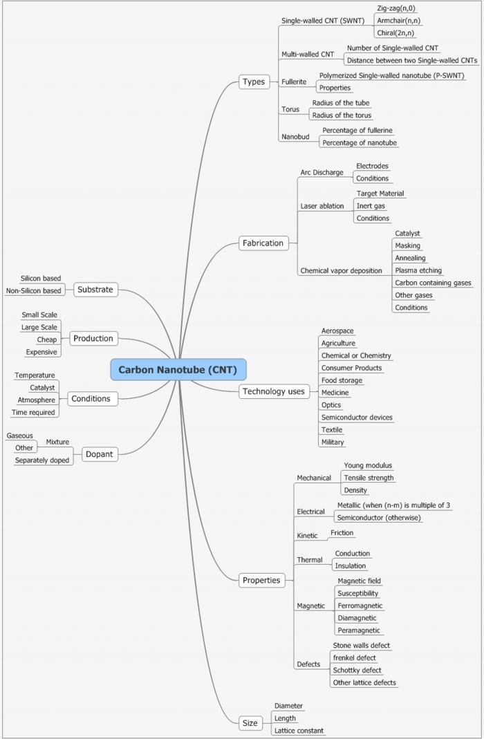
| − | + | [[Image:Carbon Nanotube1.jpg|700 px|center|thumb|Map categorization for CNT]] | |
| − | + | ||
| − | + | ||
| − | == | + | == Top ongoing projects on CNT's == |
| − | *The [http:// | + | ::* The Ajayan group is using carbon nanotubes as templates and molds for fabricating nanowires, composites, and novel ceramic fibers.[http://www.rpi.edu/locker/38/001238/INDEX.HTM] |
| + | ::* Dai group discovered how to grow nanotubes in specific directions and orientations on substrates using a chemical vapor deposition process.[http://www.stanford.edu/dept/chemistry/faculty/dai/group/] | ||
| + | ::* Smalley group is developing methods of production, purification, derivitization, analysis, and assembly of nanotubes to solve real world problems. [http://smalley.rice.edu/] | ||
| + | ::* Sun Research group is researching on polymeric nanocomposite materials based on carbon nanotubes and semiconductor and metal nanoparticles. [http://www.ces.clemson.edu/lemt/research.htm] | ||
| + | ::* Accelerator Laboratory, the University of Helsinki is researching on Ion irradiation as a tool for studying and modifying properties of carbon nanotubes.[http://beam.acclab.helsinki.fi/nanotubes/] | ||
| − | |||
| − | |||
| − | ==== | + | == IP Activity on carbon nanotubes == |
| − | + | ||
| − | + | ||
| − | + | ||
| − | + | ||
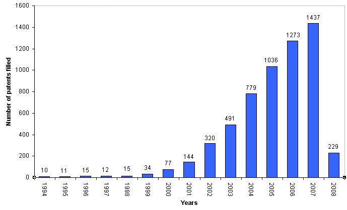
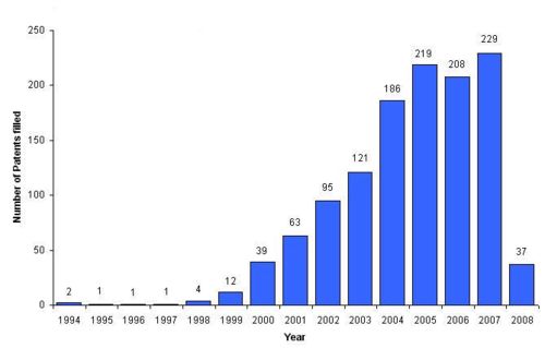
| − | + | * Number of patents filled on nanotubes are increasing exponentially by years. | |
| − | * | + | * Last year i.e 2007, around 1450 patents are filled in this field. |
| − | * | + | |
| − | + | [[Image:report11.jpg|700px|center|thumb|IP Activity by year]] | |
| − | + | ||
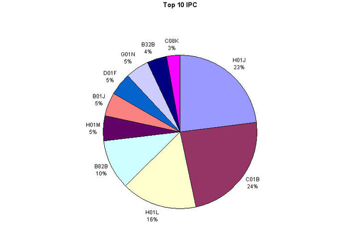
| − | + | * Major IPC classes with description is given. | |
| − | * | + | |
| − | |||
| − | |||
| − | |||
| − | |||
| − | |||
| − | + | [[Image:report3.jpg|700px|center|thumb|Top IPC]] | |
| − | + | ||
| − | + | ||
| − | |||
| + | {|border="2" cellspacing="0" cellpadding="4" width="100%" | ||
| + | |align = "center" bgcolor = "#C0C0C0"|S. no. | ||
| + | |align = "center" bgcolor = "#C0C0C0"|IPC Classification | ||
| + | |align = "center" bgcolor = "#C0C0C0"|Description | ||
| + | |- | ||
| + | |align = "center"|1 | ||
| + | |align = "center"|H01J | ||
| + | |align = "center"|ELECTRIC DISCHARGE TUBES OR DISCHARGE LAMPS | ||
| + | |- | ||
| + | |align = "center"|2 | ||
| + | |align = "center"|C01B | ||
| + | |align = "center"|NON-METALLIC ELEMENTS AND THEIR COMPOUNDS | ||
| + | |- | ||
| + | |align = "center"|3 | ||
| + | |align = "center"|H01L | ||
| + | |align = "center"|SEMICONDUCTOR DEVICES AND ELECTRIC SOLID STATE DEVICES | ||
| + | |- | ||
| + | |align = "center"|4 | ||
| + | |align = "center"|B82B | ||
| + | |align = "center"|NANOTECHNOLOGY | ||
| + | |- | ||
| + | |align = "center"|5 | ||
| + | |align = "center"|H01M | ||
| + | |align = "center"|BATTERIES OR FOR THE DIRECT CONVERSION OF CHEMICAL ENERGY INTO ELECTRICAL ENERGY | ||
| + | |- | ||
| + | |align = "center"|6 | ||
| + | |align = "center"|B01J | ||
| + | |align = "center"|CHEMICAL OR PHYSICAL PROCESSES, e.g. CATALYSIS, COLLOID CHEMISTRY AND THEIR RELEVANT APPARATUS | ||
| + | |- | ||
| + | |align = "center"|7 | ||
| + | |align = "center"|D01F | ||
| + | |align = "center"|CHEMICAL FEATURES IN THE MANUFACTURE OF ARTIFICIAL FILAMENTS, THREADS, FIBRES, BRISTLES, OR RIBBONS AND APPARATUS SPECIALLY ADAPTED FOR THE MANUFACTURE OF CARBON FILAMENTS | ||
| + | |- | ||
| + | |align = "center"|8 | ||
| + | |align = "center"|G01N | ||
| + | |align = "center"|INVESTIGATING OR ANALYSING MATERIALS BY DETERMINING THEIR CHEMICAL OR PHYSICAL PROPERTIES | ||
| + | |- | ||
| + | |align = "center"|9 | ||
| + | |align = "center"|B32B | ||
| + | |align = "center"|LAYERED PRODUCTS, i.e. PRODUCTS BUILT-UP OF STRATA OF FLAT OR NON-FLAT, e.g. CELLULAR OR HONEYCOMB, FORM | ||
| + | |- | ||
| + | |align = "center"|10 | ||
| + | |align = "center"|C08K | ||
| + | |align = "center"|USE OF INORGANIC OR NON-MACROMOLECULAR ORGANIC SUBSTANCES AS COMPOUNDING INGREDIENTS | ||
| + | |- | ||
| + | |} | ||
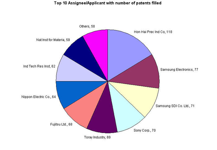
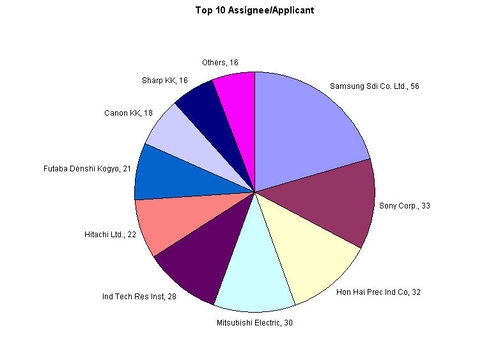
| − | == | + | * Hon Hai Prec Ind Co leads the number of patent filing by a great margin with their competitors. |
| − | === | + | * Samsung Electronics and Samsung SDI Co. Ltd. together contributes 148 patents. |
| − | {|border="2" cellspacing="0" cellpadding="4" width="100%" align=" | + | |
| − | |bgcolor = "# | + | |
| − | |bgcolor = "# | + | [[Image:report4.jpg|700px|center|thumb|Top Assignee]] |
| − | |bgcolor = "# | + | |
| − | |bgcolor = "# | + | == Sample Analysis == |
| + | * Below is the link for sample spreadsheet analysis for Carbon nanotubes. | ||
| + | |||
| + | [[Media:Sample taxomomy for carbon nano tubes.xls|Sample analysis on carbon nanotubes]] | ||
| + | |||
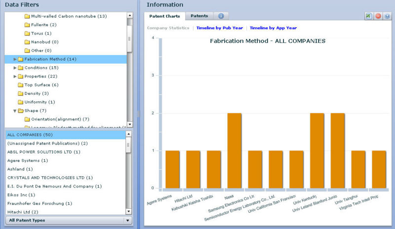
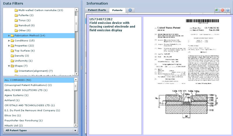
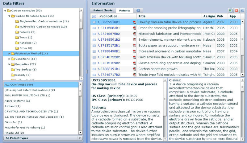
| + | == Dashboard == | ||
| + | === Dashboard Snapshots === | ||
| + | |||
| + | [[Image:dashboard1.jpg|center|800px]] | ||
| + | |||
| + | |||
| + | [[Image:dashboard2.jpg|center|800px]] | ||
| + | |||
| + | |||
| + | [[Image:dashboard3.jpg|center|800px]] | ||
| + | |||
| + | === Link to Dashboard === | ||
| + | [http://client.dolcera.com/dashboard/dashboard.html?workfile_id=274 Dashboard for CNTs] | ||
| + | |||
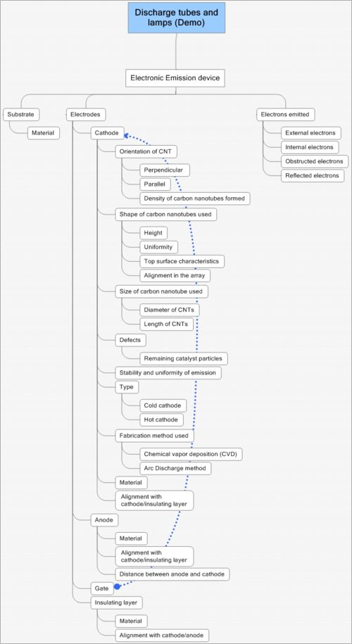
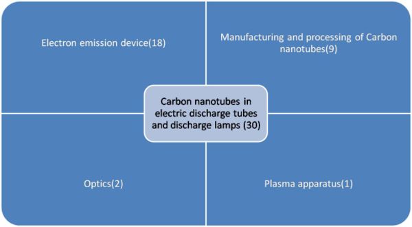
| + | == Carbon nanotube in Electric discharge tubes and discharge lamps (IPC H01J) == | ||
| + | |||
| + | === IP Map === | ||
| + | |||
| + | [[Image:Discharge lamps.jpg|500px|center|thumb|Map for electron emitter devices]] | ||
| + | |||
| + | === IP Activity on carbon nanotubes in Electric discharge tubes and discharge lamps === | ||
| + | |||
| + | |||
| + | [[Image:report6.jpg|500 px|center|thumb|IP activity by year]] | ||
| + | |||
| + | [[Image:report5.jpg|500 px|center|thumb|Top Assignee]] | ||
| + | |||
| + | === Analysis === | ||
| + | |||
| + | {|border="2" cellspacing="0" cellpadding="4" width="100%" | ||
| + | |align = "justify" bgcolor = "#C0C0C0"|'''S.no''' | ||
| + | |align = "justify" bgcolor = "#C0C0C0"|'''Patent/Publication No.''' | ||
| + | |align = "justify" bgcolor = "#C0C0C0"|'''Assignee / Applicant''' | ||
| + | |align = "justify" bgcolor = "#C0C0C0"|'''Title''' | ||
| + | |align = "justify" bgcolor = "#C0C0C0"|'''Description of the device''' | ||
| + | |align = "justify" bgcolor = "#C0C0C0"|'''Use of CNT in it''' | ||
| + | |align = "justify" bgcolor = "#C0C0C0"|'''Technology Area''' | ||
|- | |- | ||
| − | | | + | |align = "justify" bgcolor = "#C0C0C0"|1 |
| − | | | + | |align = "justify"|[http://patft.uspto.gov/netacgi/nph-Parser?Sect1=PTO1&Sect2=HITOFF&d=PALL&p=1&u=%2Fnetahtml%2FPTO%2Fsrchnum.htm&r=1&f=G&l=50&s1=7336028.PN.&OS=PN/7336028&RS=PN/7336028 US7336028B2] |
| − | | | + | |align = "justify"|Samsung SDI Co., Ltd. |
| − | | | + | |align = "justify"|Electron emission device having multi-layered gate electrode structure |
| + | |align = "justify"|A multilayered electron emission device is described with a predetermined gap between the electrodes. | ||
| + | |align = "justify"|Electron emission sources can be made up of CNTs. | ||
| + | |align = "justify"|Electron emission device | ||
|- | |- | ||
| − | | | + | |align = "justify" bgcolor = "#C0C0C0"|2 |
| − | | | + | |align = "justify"|US7315129B2 |
| − | | | + | |align = "justify"|Semiconductor Energy Laboratory Co., Ltd. |
| − | | | + | |align = "justify"|Plasma producing apparatus and doping apparatus |
| + | |align = "justify"|A plasma chamber anad plasma appratus is described with two electrodes and sustrate and CNTs. | ||
| + | |align = "justify"|CNTs are on the surface of the cathode electrode. | ||
| + | |align = "justify"|Plasma Appratus | ||
|- | |- | ||
| − | | | + | |align = "justify" bgcolor = "#C0C0C0"|3 |
| − | | | + | |align = "justify"|[http://patft.uspto.gov/netacgi/nph-Parser?Sect1=PTO1&Sect2=HITOFF&d=PALL&p=1&u=%2Fnetahtml%2FPTO%2Fsrchnum.htm&r=1&f=G&l=50&s1=7307432.PN.&OS=PN/7307432&RS=PN/7307432 US7307432B2] |
| − | | | + | |align = "justify"|Yokogawa Electric Corporation |
| − | | | + | |align = "justify"|Electron beam generating apparatus and optical sampling apparatus using the same |
| + | |align = "justify"|Optical sampling appratus with electrodes with deflection electrode and charge detection section. | ||
| + | |align = "justify"|Cathode is comprising of carbon nanotubes. | ||
| + | |align = "justify"|Optical sampling appratus. | ||
|- | |- | ||
| − | | | + | |align = "justify" bgcolor = "#C0C0C0"|4 |
| − | | | + | |align = "justify"|[http://patft.uspto.gov/netacgi/nph-Parser?Sect1=PTO1&Sect2=HITOFF&d=PALL&p=1&u=%2Fnetahtml%2FPTO%2Fsrchnum.htm&r=1&f=G&l=50&s1=7306503.PN.&OS=PN/7306503&RS=PN/7306503 US7306503B2] |
| − | | | + | |align = "justify"|Canon Kabushiki Kaisha |
| − | | | + | |align = "justify"|Method and apparatus of fixing carbon fibers on a substrate using an aerosol deposition process |
| + | |align = "justify"|Appratus for manufacturing substate with carbon nanotubes in it. | ||
| + | |align = "justify"|Arc dischage method is involved for producing CNTs and hence forming it on substrate. | ||
| + | |align = "justify"|Manufacturing and Processing of CNT<nowiki>’</nowiki>s | ||
|- | |- | ||
| − | | | + | |align = "justify" bgcolor = "#C0C0C0"|5 |
| − | | | + | |align = "justify"|[http://patft.uspto.gov/netacgi/nph-Parser?Sect1=PTO1&Sect2=HITOFF&d=PALL&p=1&u=%2Fnetahtml%2FPTO%2Fsrchnum.htm&r=1&f=G&l=50&s1=7259510.PN.&OS=PN/7259510&RS=PN/7259510 US7259510B1] |
| − | | | + | |align = "justify"|Agere Systems Inc. |
| − | | | + | |align = "justify"|On-chip vacuum tube device and process for making device |
| + | |align = "justify"|Microwave vacuum tube is described with electrodes and CNTs. | ||
| + | |align = "justify"|Cathode is comprising of carbon nanotubes. | ||
| + | |align = "justify"|Electron emission device | ||
|- | |- | ||
| − | | | + | |align = "justify" bgcolor = "#C0C0C0"|6 |
| + | |align = "justify"|[http://patft.uspto.gov/netacgi/nph-Parser?Sect1=PTO1&Sect2=HITOFF&d=PALL&p=1&u=%2Fnetahtml%2FPTO%2Fsrchnum.htm&r=1&f=G&l=50&s1=7232987.PN.&OS=PN/7232987&RS=PN/7232987 US7232987B2] | ||
| + | |align = "justify"|None | ||
| + | |align = "justify"|Instrument and method to measure available light energy for photosynthesis | ||
| + | |align = "justify"|A device to calculate and filter amout of light required and available for photosynthesis of plants. | ||
| + | |align = "justify"|Photovoltaic material is made up of carbon nanotubes. | ||
| + | |align = "justify"|Optical Instrument | ||
| + | |- | ||
| + | |align = "justify" bgcolor = "#C0C0C0"|7 | ||
| + | |align = "justify"|[http://patft.uspto.gov/netacgi/nph-Parser?Sect1=PTO1&Sect2=HITOFF&d=PALL&p=1&u=%2Fnetahtml%2FPTO%2Fsrchnum.htm&r=1&f=G&l=50&s1=7161148.PN.&OS=PN/7161148&RS=PN/7161148 US7161148B1] | ||
| + | |align = "justify"|Crystals and Technologies, Ltd. | ||
| + | |align = "justify"|Tip structures, devices on their basis, and methods for their preparation | ||
| + | |align = "justify"| A tip structure for an electron emissive device or a scanning probe device is described. | ||
| + | |align = "justify"|At least one link of the tip structure is made up of Carbon naotubes. | ||
| + | |align = "justify"|Electron emission device | ||
| + | |- | ||
| + | |align = "justify" bgcolor = "#C0C0C0"|8 | ||
| + | |align = "justify"|[http://patft.uspto.gov/netacgi/nph-Parser?Sect1=PTO1&Sect2=HITOFF&d=PALL&p=1&u=%2Fnetahtml%2FPTO%2Fsrchnum.htm&r=1&f=G&l=50&s1=7175494.PN.&OS=PN/7175494&RS=PN/7175494 US7175494B1] | ||
| + | |align = "justify"|cDream Corporation | ||
| + | |align = "justify"|Forming carbon nanotubes at lower temperatures suitable for an electron-emitting device | ||
| + | |align = "justify"|An electron emission device is described comprising of carbon nanotubes. | ||
| + | |align = "justify"|Carbon nanotubes are manufactured at 300° C. to 500° C which makes them compatible with the thermal stress of the underlying substrate. | ||
| + | |align = "justify"|Electron emission device | ||
| + | |- | ||
| + | |align = "justify" bgcolor = "#C0C0C0"|9 | ||
| + | |align = "justify"|[http://patft.uspto.gov/netacgi/nph-Parser?Sect1=PTO1&Sect2=HITOFF&d=PALL&p=1&u=%2Fnetahtml%2FPTO%2Fsrchnum.htm&r=1&f=G&l=50&s1=7161286.PN.&OS=PN/7161286&RS=PN/7161286 US7161286B2] | ||
| + | |align = "justify"|Tsinghua University <nowiki>|</nowiki> Hon Hai Precision Ind. Co., Ltd. | ||
| + | |align = "justify"|Carbon nanotube array and method for making same | ||
| + | |align = "justify"|A carbon nanotube-based device is described which includes a substrate and number of catalytic nano-sized particles. | ||
| + | |align = "justify"|Carbon nanotubes are manufactured on the substrate. | ||
| + | |align = "justify"|Manufacturing and Processing of CNT<nowiki>’</nowiki>s | ||
| + | |- | ||
| + | |align = "justify" bgcolor = "#C0C0C0"|10 | ||
| + | |align = "justify"|[http://patft.uspto.gov/netacgi/nph-Parser?Sect1=PTO1&Sect2=HITOFF&d=PALL&p=1&u=%2Fnetahtml%2FPTO%2Fsrchnum.htm&r=1&f=G&l=50&s1=7145528.PN.&OS=PN/7145528&RS=PN/7145528 US7145528B2] | ||
| + | |align = "justify"|Canon Kabushiki Kaisha | ||
| + | |align = "justify"|Display device and driving and controlling method therefor | ||
| + | |align = "justify"|A display device with display panel is described and use of electron emitters. | ||
| + | |align = "justify"|Cathode is comprising of carbon nanotubes. | ||
| + | |align = "justify"|Electron emission device | ||
| + | |- | ||
| + | |align = "justify" bgcolor = "#C0C0C0"|11 | ||
| + | |align = "justify"|[http://patft.uspto.gov/netacgi/nph-Parser?Sect1=PTO1&Sect2=HITOFF&d=PALL&p=1&u=%2Fnetahtml%2FPTO%2Fsrchnum.htm&r=1&f=G&l=50&s1=7115863.PN.&OS=PN/7115863&RS=PN/7115863 US7115863B1] | ||
| + | |align = "justify"|Hitachi, Ltd. | ||
| + | |align = "justify"|Probe for scanning probe lithography and making method thereof | ||
| + | |align = "justify"|A probe of scanning probe lithography is described | ||
| + | |align = "justify"|Shaft of the probe is made up of Carbon nanaotubes. | ||
| + | |align = "justify"|Manufacturing and Processing of CNT<nowiki>’</nowiki>s | ||
| + | |- | ||
| + | |} | ||
| − | |||
| − | === | + | [[Media:Analysis_electrical.xls|Sample Analysis on use of Carbon nanotubes in discharge tubes and discharge lamps]] |
| − | {|border="2" cellspacing="0" cellpadding="4" width="100% | + | |
| − | |align = "center" bgcolor = "# | + | |
| − | |align = "center" bgcolor = "# | + | [[Image:Analysis1.jpg|600px|center|thumb|Sample Analysis for discharge tubes and discharge lamps patents(30 patents)]] |
| − | + | ||
| − | + | == Key Players == | |
| − | + | === Universities === | |
| + | * Universities play an important role in research and that's why it needs to be analyzed. | ||
| + | * Only 245 patents are filled by the universities research division. | ||
| + | * But companies are dependent on them for research activities. | ||
| + | * The analysis will give the insight of most involved university in terms of research on Carbon nanotubes. | ||
| + | |||
| + | [[Image:report2.jpg|700 px|center|Top Universities|thumb|Number of patents by universities in Carbon nanotubes area]] | ||
| + | |||
| + | === Companies === | ||
| + | |||
| + | * Large number of companies are now moving into this area. | ||
| + | * Number of startups are coming into the picture. | ||
| + | |||
| + | {|border="2" cellspacing="0" cellpadding="4" width="100%" | ||
| + | |align = "center" bgcolor = "#C0C0C0"|Top Companies | ||
| + | |align = "center" bgcolor = "#C0C0C0"|Number of patents filled | ||
|- | |- | ||
| − | |align = "center | + | |align = "center"|[http://www.foxconn.com/ Hon Hai Prec Ind Co] |
| − | + | |align = "center"|118 | |
| − | + | ||
| − | |align = "center"| | + | |
| − | + | ||
|- | |- | ||
| − | |align = "center" | + | |align = "center"|[http://www.samsung.com Samsung Electronics] |
| − | | | + | |align = "center"|77 |
| − | |align = "center"| | + | |
| − | + | ||
|- | |- | ||
| − | |align = "center | + | |align = "center"|[http://www.samsungsdi.com/contents/kr/main.jsp Samsung SDI Co. Ltd.] |
| − | |align = "center"| | + | |align = "center"|71 |
| − | + | ||
| − | + | ||
|- | |- | ||
| − | | | + | |align = "center"|[http://www.sony.com Sony Corp.] |
| + | |align = "center"|70 | ||
| + | |- | ||
| + | |align = "center"|[http://www.toray.com/ Toray Industry] | ||
| + | |align = "center"|69 | ||
| + | |- | ||
| + | |align = "center"|[http://www.fujitsu.com/global/ Fujitsu Ltd.] | ||
| + | |align = "center"|68 | ||
| + | |- | ||
| + | |align = "center"|[http://www.nec.com/ Nippon Electric Co.] | ||
| + | |align = "center"|64 | ||
| + | |- | ||
| + | |align = "center"|[http://www.itri.org.tw/eng/research/nano/index.jsp Ind Tech Res Inst] | ||
| + | |align = "center"|62 | ||
| + | |- | ||
| + | |align = "center"|[http://www.imm.ac.cn/en/index.html Nat Inst for Materia] | ||
| + | |align = "center"|59 | ||
| + | |- | ||
| + | |align = "center"|Others | ||
| + | |align = "center"|58 | ||
| + | |- | ||
| + | |} | ||
| − | |||
| − | |||
| − | |||
| − | |||
| − | + | == Market Research == | |
| + | === Nanotechnology market === | ||
| + | * Nanotechnology is a growing market. | ||
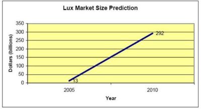
| + | * Lux Research (a market research company in nanotechnology) believes that market will reach from $13 billion in 2005 to $292 billion in 2010. | ||
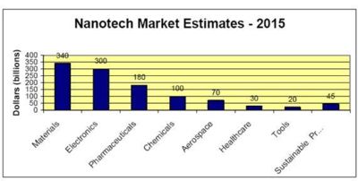
| + | * In 2015 market for nano materials will reach to $340 billion and electronics market will reach to $300 billion. | ||
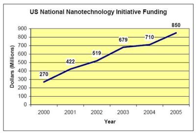
| + | * US nanotech funding has increased from $270 million to $850 million. | ||
| − | + | [[Image:lux1.jpg|400 px|center|thumb|Predictions of market by Lux research]] | |
| − | |||
| − | |||
| − | |||
| − | [[Image: | + | [[Image:lux3.jpg|400 px|center|thumb|US funding]] |
| − | |||
| − | + | [[Image:lux2.jpg|400 px|center|thumb|Market by different categories]] | |
| − | + | ||
| − | + | ||
| − | + | === Carbon Nanotubes market === | |
| − | + | ||
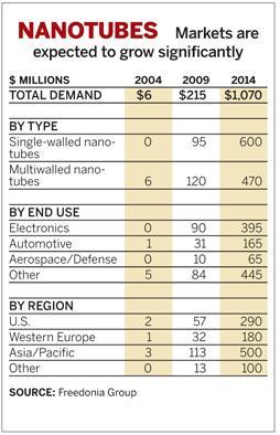
| − | + | * Market size will increase from $6 million in 2004 to $1,070 million in 2014. | |
| − | == | + | |
| + | [[Image:marketresearch.jpg|300 px|center|thumb|Carbon nanotubes market estimate]] | ||
| + | |||
| + | == Published Papers == | ||
| + | * Academic papers published on carbon nanotubes have been on the rise and patent filings have been keeping up with this upswing, says a review in the journal Science. | ||
| + | * According to the review, around 1,500 scientific papers were published in 2001 compared to about 1,100 in 2000 and around 700 in 1999. | ||
| + | |||
| + | [http://news.thomasnet.com/IMT/archives/2002/09/materials_nanot.html?t=archive Source] | ||
| + | |||
| + | |||
| + | |||
| + | == SWOT analysis on nanotechnology == | ||
{|border="2" cellspacing="0" cellpadding="4" width="100%" | {|border="2" cellspacing="0" cellpadding="4" width="100%" | ||
| − | |align = "center" bgcolor = "# | + | |align = "center" bgcolor = "#D99795"|'''Strength''' |
| − | |align = "center" bgcolor = "# | + | |align = "center" bgcolor = "#D99795"|'''Weakness''' |
| − | + | ||
| − | + | ||
| − | + | ||
|- | |- | ||
| − | |align = "center | + | |align = "center"|In nanomaterials research and development |
| − | |align = "center"| | + | |align = "center"|Critical issues(ecological meltdown,poverty and disease) |
| − | + | ||
| − | + | ||
| − | + | ||
|- | |- | ||
| − | |align = "center" bgcolor = "# | + | |align = "center" bgcolor = "#DBEEF3"|In biomimetics research |
| − | |align = "center" | + | |align = "center" bgcolor = "#DBEEF3"|Lack of planet friendly scorecard for research |
| − | | | + | |
| − | + | ||
| − | + | ||
|- | |- | ||
| − | |align = "center | + | |align = "center"|In nanoelectronics and IT research including quantum computing |
| − | |align = "center"| | + | |align = "center"|No clear technology transfer routes to the less developed world. |
| − | + | ||
| − | + | ||
| − | + | ||
|- | |- | ||
| − | |align = "center" bgcolor = "# | + | |align = "center" bgcolor = "#DBEEF3"|In nanophotovoltaic research |
| − | |align = "center" | + | |align = "center" bgcolor = "#DBEEF3"|Fragmented research infrastructure |
| − | | | + | |
| − | + | ||
| − | + | ||
|- | |- | ||
| − | |align = "center | + | |align = "center"|In nanosensors research and development |
| − | |align = "center"| | + | |align = "center"|Nationally variable industry pull through |
| − | + | ||
| − | + | ||
| − | + | ||
|- | |- | ||
| − | |align = "center" bgcolor = "# | + | |align = "center" bgcolor = "#DBEEF3"|In strong industrial base in instrumentation |
| − | |align = "center" | + | |align = "center" bgcolor = "#DBEEF3"|Variable incentives/cultures for supporting start-ups |
| − | + | ||
| − | + | ||
| − | + | ||
|- | |- | ||
| − | |align = "center | + | |align = "center"|In nanomedicine |
| − | |align = "center"| | + | |align = "center"|Funding slow and bureaucratic |
| − | + | ||
| − | + | ||
| − | + | ||
|- | |- | ||
| − | |align = "center" bgcolor = "# | + | |align = "center" bgcolor = "#DBEEF3"|In cultural differences resulting in imaginative approaches to results |
| − | |align = "center" | + | |align = "center" bgcolor = "#DBEEF3"|No wide support for individual genius |
| − | | | + | |
| − | + | ||
| − | + | ||
|- | |- | ||
| − | |align = "center | + | |align = "center"|In the ability to work in teams |
| − | |align = "center"| | + | |align = "center"|Academic research often lags industry |
| − | + | ||
| − | + | ||
| − | + | ||
|- | |- | ||
| − | |align = "center" bgcolor = "# | + | |align = "center" bgcolor = "#DBEEF3"|Acceleration of new company formation underway |
| − | |align = "center" | + | |align = "center" bgcolor = "#DBEEF3"|Funding may be duplicated |
| − | | | + | |
| − | + | ||
| − | + | ||
|- | |- | ||
| + | |align = "center"|Openness in developing and adopting environmentally friendly techniques | ||
| + | |align = "center"|Lack of fiscal incentives for environmentally friendly techniques;also lack of legal incentives | ||
| + | |||
| + | |- | ||
| + | |align = "center" bgcolor = "#DBEEF3"|Openness to developing technologies for the less developed regions | ||
| + | |align = "center" bgcolor = "#DBEEF3"|Critically slow emergence of technology from the research base | ||
| + | |||
| + | |- | ||
| + | |align = "center"| | ||
| + | |align = "center"|Lack of skilled staff | ||
| + | |||
| + | |- | ||
| + | |align = "center" bgcolor = "#D99795"|'''Opportunities''' | ||
| + | |align = "center" bgcolor = "#D99795"|'''Threats''' | ||
| + | |||
| + | |- | ||
| + | |align = "center"|The exploitation of planet and people friendly research | ||
| + | |align = "center"|Brain drain in life sciences,electronics,software and engineering | ||
| + | |||
| + | |- | ||
| + | |align = "center" bgcolor = "#DBEEF3"|Development of widely available technologies(sensors,renewable energy,medicine etc.) | ||
| + | |align = "center" bgcolor = "#DBEEF3"|Public backlash to nanotechnology | ||
| + | |||
| + | |- | ||
| + | |align = "center"|Creation of new technologies(medical and non-medical) | ||
| + | |align = "center"|Too little,too late, of the technologies that matter | ||
| + | |||
| + | |- | ||
| + | |align = "center" bgcolor = "#DBEEF3"|Reduction animal experimentation through cell-base toxicity testing | ||
| + | |align = "center" bgcolor = "#DBEEF3"| | ||
| + | |||
| + | |- | ||
| + | |align = "center"|Critical niche opportunities in areas such as lab-on-a-chip and sensor technology | ||
| + | |align = "center"| | ||
| + | |||
|} | |} | ||
| + | == Conferences == | ||
| − | + | * Major Conferences | |
| − | |||
| − | |||
| − | == | + | {|border="2" cellspacing="0" cellpadding="4" width="100%" |
| + | |align = "center" bgcolor = "#C0C0C0"|'''S.no.''' | ||
| + | |align = "center" bgcolor = "#C0C0C0"|'''Conference''' | ||
| + | |align = "center" bgcolor = "#C0C0C0"|'''Location''' | ||
| + | |align = "center" bgcolor = "#C0C0C0"|'''Date''' | ||
| + | |align = "center" bgcolor = "#C0C0C0"|'''Email''' | ||
| + | |- | ||
| + | |align = "right" bgcolor = "#C0C0C0"|1 | ||
| + | |<font color="#0000FF"><u>[http://www.nsti.org/Nanotech2008/ Nanotech 2008 - 11th Annual NSTI Nanotechnology Conference and Trade Show]</u></font> | ||
| + | |Boston,USA | ||
| + | |1-5June, 2008 | ||
| + | |bfr@nsti.org | ||
| + | |- | ||
| + | |align = "right" bgcolor = "#C0C0C0"|2 | ||
| + | |<font color="#0000FF"><u>[http://www.nanoeurope.com/ NanoEurope 2008]</u></font> | ||
| + | |St.Gallen, Switzerland | ||
| + | |16-17 Sep, 2008 | ||
| + | |joerg.guettinger@ncb.ch | ||
| + | |- | ||
| + | |align = "right" bgcolor = "#C0C0C0"|3 | ||
| + | |<font color="#0000FF"><u>[http://www.nanotech.net/node/2 Nanotech Northern Europe 2008]</u></font> | ||
| + | |Copenhagen,Denmark | ||
| + | |23-25 Sep, 2008 | ||
| + | |katriina.forsstrom@spinverse.com | ||
| + | |- | ||
| + | |} | ||
| − | + | * Complete list of Nanotechnology Conferences | |
| + | http://www.allconferences.com/Science/Nanotechnology/ | ||
| − | ''' | + | |
| − | ''' | + | ==Contact Dolcera== |
| − | + | ||
| − | + | {| style="border:1px solid #AAA; background:#E9E9E9" align="center" | |
| − | + | |- | |
| + | ! style="background:lightgrey" | Samir Raiyani | ||
| + | |- | ||
| + | | '''Email''': [mailto:info@dolcera.com info@dolcera.com] | ||
| + | |- | ||
| + | | '''Phone''': +1-650-269-7952 | ||
| + | |} | ||
Revision as of 00:21, 30 April 2009
Contents
- 1 Introduction
- 2 Carbon Nanotubes
- 3 Application of Carbon nanotubes
- 4 Top ongoing projects on CNT's
- 5 IP Activity on carbon nanotubes
- 6 Sample Analysis
- 7 Dashboard
- 8 Carbon nanotube in Electric discharge tubes and discharge lamps (IPC H01J)
- 9 Key Players
- 10 Market Research
- 11 Published Papers
- 12 SWOT analysis on nanotechnology
- 13 Conferences
- 14 Contact Dolcera
Introduction
Nanotechnology
Nanotechnology refers broadly to a field of applied science and technology whose unifying theme is the control of matter on the atomic and molecular scale, normally 1 to 100 nanometers, and the fabrication of devices with critical dimensions that lie within that size range.
Run of Nanotechnology
- December 29, 1959: The first thought of Nanotechnology was given by Richard Feynman in "There's Plenty of Room at the Bottom" at an American Physical Society meeting at Caltech.
- September, 1981: First technical paper published on molecular nanotechnology. The same year scanning tunneling microscope (STM) invented.
- 1982-1990:Books and prizes on nanotechnology. Atomic force microscope invented in 1986.
- 1991: Carbon Nanotubes (CNT's) discovered.
- 1997: First company on nanotechnology founded, it's name is Zyvex.
- 1998-2007: Research, investment, conferences and meetings on nanotechnology.
Applications of Nanotechnology
It has or will have applications in almost all areas we can think of.
| Environment and Energy | Medical and Health | Electronics and Computers | Space, Aircraft and Transportation | Materials and Manufacturing |
|---|---|---|---|---|
|
|
|
|
|
- Aerospace
- Medicine
- Identifying location of cancer cells. [1]
- Delivering chemotherapy drugs directly to cancer cells.[2]
- Nanoshells that concentrate the heat from infrared light to destroy cancer cells with minimal damage to surrounding healthy cells. [3]
- Nanotubes used in broken bones to provide a structure for new bone material to grow.[4]
- Nanoparticles that can attach to cells infected with various diseases and allow a lab to identify, in a blood sample, the particular disease.[5]
- Food Storage
- Clay nanocomposites are being used to provide an impermeable barrier to gasses such as oxygen or carbon dioxide in lightweight bottles, cartons and packaging films.
- Food storage bins are being produced with silver nanoparticles embedded in the plastic. The silver nanoparticles kill bacteria from any food that was previously stored in the bins, minimizing health risks from harmful bacteria.[6]
- It is possible to use nanosensors in plastic packaging to detect gases given off by food when it spoils. The packaging itself changes color to alert you to food gone bad.
- Agriculture
- Food will be more tastier and healthier using nanaotechnology.[7]
- Research is also being conducted to develop nanocapsules containing nutrients that would be released when nanosensors detect a vitamin deficiency in your body.
- Researchers are also working on pesticides encapsulated in nanoparticles; that only release pesticide within an insect’s stomach, minimizing the contamination of plants themselves.
- Another development being persued is a network of nanosensors and dispensers used throughout a food crop. The sensors recognize when a plant needs nutrients or water, before there is any sign that the plant is deficient. The dispensers then release fertilizer, nutrients, or water as needed, optimizing the growth of each plant in the field one by one.
- Chemistry
- Semiconductor devices
- Optics
- The first sunglasses using protective and antireflective ultrathin polymer coatings are on the market.
- Nanotechnology also offers scratch resistant surface coatings based on nanocomposites.
- Nano-optics could allow for an increase in precision of pupil repair and other types of laser eye surgery.
- Textile
- The use of engineered nanofibers already makes clothes water- and stain-repellent or wrinkle-free.
- Textiles with a nanotechnological finish can be washed less frequently and at lower temperatures.
- Nanotechnology has been used to integrate tiny carbon particles membrane and guarantee full-surface protection from electrostatic charges for the wearer.
- Consumer products
- Nanotechnology is now entered in almost all consumer products,for details see [11]
Carbon Nanotubes
Carbon Nanotubes (CNT's) are cylindrical shaped allotrope of carbon with length to diameter ratio exceeding 1,000,000.
Such cylindrical carbon molecules have novel properties that make them potentially useful in many applications in nanotechnology, electronics, optics and other fields of materials science. They exhibit extraordinary strength and unique electrical properties, and are efficient conductors of heat.
Types
- Single-walled CNT's: This type of nanotube can be formed by rolling Graphene sheet. Graphene is a single planar sheet of sp²-bonded carbon atoms that are densely packed in a honeycomb crystal lattice. Types of Single-walled CNT's:
- Zig-zag(n,0)
- Armchair(n,n)
- Chiral(2n,n)
- Multi-walled: Multi-walled nanotubes(MWNT) consist of multiple layers of graphite rolled in on themselves to form a tube shape.
- Fullerite: Fullerites are the solid-state manifestation of fullerenes and related compounds and materials. Being highly incompressible nanotube forms, polymerized single-walled nanotubes (P-SWNT) are a class of fullerites and are comparable to diamond in terms of hardness.
- Torus: A nanotorus is a theoretically described carbon nanotube bent into a torus (doughnut shape).
- Nanobud: The material fullerene-like "buds" are covalently bonded to the outer sidewalls of the underlying carbon nanotube. This hybrid material has useful properties of both fullerenes and carbon nanotubes.
Properties
- Physical Properties
| Material | Young’s modulus (GPa) | Tensile Strength (GPa) | Density (g/cm3) |
| Single wall nanotube | 1054 | 150 | N/A |
| Multi wall nanotube | 1200 | 150 | 2.6 |
| Steel | 208 | 0.4 | 7.8 |
| Epoxy | 3.5 | 0.005 | 1.25 |
| Wood | 16 | 0.008 | 0.6 |
- Electrical Properties: Because of the symmetry and unique electronic structure of graphene, the structure of a nanotube strongly affects its electrical properties. For a given (n,m) nanotube, if n − m is a multiple of 3, then the nanotube is metallic, otherwise the nanotube is a semiconductor. Thus all armchair (n=m) nanotubes are metallic, and nanotubes (5,0), (6,4), (9,1), etc. are semiconducting. In theory, metallic nanotubes can have an electrical current density more than 1,000 times greater than metals such as silver and copper.
Method of fabrication
- Arc discharge: It is the simplest and most commonly used method of producing Carbon nanotubes. This method creates CNTs through arc-vaporization of two carbon rods placed end to end, separated by approximately 1mm, in an enclosure that is usually filled with inert gas (helium, argon) at low pressure (between 50 and 700 mbar).
- Laser ablation: In 1996, a dual-pulsed laser vaporization technique was developed, which produced SWNTs in gram quantities and yields of >70wt% purity. Samples were prepared by laser vaporization of graphite rods with a 50:50 catalyst mixture of Co and Ni (particle size ~1um) at 1200oC in flowing argon, followed by heat treatment in a vacuum at 1000oC to remove the C60 and other fullerenes.
- Chemical vapor deposition (CVD):Large amounts of CNTs can be formed by catalytic CVD of acetylene over Co and Fe catalysts supported on silica or zeolite.
Application of Carbon nanotubes
- Polymer Composites: The first realized major commercial application of MWNTs is their use as electrically conducting components in polymer composites.Depending on the polymer matrix, conductivities of 0.01 to 0.1 S/cm can be obtained for 5% loading; much lower conductivity levels suffice for dissipating electrostatic charge. The low loading levels and the nanofiber morphology of the MWNTs allow electronic conductivity to be achieved while avoiding or minimizing degradation of other performance aspects, such as mechanical properties and the low melt flow viscosity needed for thin-wall molding applications.
- Electrochemical devices: Because of the high electrochemically accessible surface area of porous nanotube arrays, combined with their high electronic conductivity and useful mechanical properties, these materials are attractive as electrodes for devices that use electrochemical double-layer charge injection.
- Hydrogen storage: Nanotubes have been long heralded as potentially useful for hydrogen storage (for example, for fuel cells that power electric vehicles or laptop computers).
- Field emission devices: Industrial and academic research activity on electronic devices has focused principally on using SWNTs and MWNTs as field emission electron sources for flat panel displays, lamps, gas discharge tubes providing surge protection, and x-ray and microwave generators.
- Nanometer-sized electronic devices:
- Sensors and probes: Possible chemical sensor applications of nonmetallic nanotubes are interesting, because nanotube electronic transport and thermopower (voltages between junctions caused by interjunction temperature differences) are very sensitive to substances that affect the amount of injected charge.The main advantages are the minute size of the nanotube sensing element and the correspondingly small amount of material required for a response.
Top ongoing projects on CNT's
- The Ajayan group is using carbon nanotubes as templates and molds for fabricating nanowires, composites, and novel ceramic fibers.[12]
- Dai group discovered how to grow nanotubes in specific directions and orientations on substrates using a chemical vapor deposition process.[13]
- Smalley group is developing methods of production, purification, derivitization, analysis, and assembly of nanotubes to solve real world problems. [14]
- Sun Research group is researching on polymeric nanocomposite materials based on carbon nanotubes and semiconductor and metal nanoparticles. [15]
- Accelerator Laboratory, the University of Helsinki is researching on Ion irradiation as a tool for studying and modifying properties of carbon nanotubes.[16]
IP Activity on carbon nanotubes
- Number of patents filled on nanotubes are increasing exponentially by years.
- Last year i.e 2007, around 1450 patents are filled in this field.
- Major IPC classes with description is given.
| S. no. | IPC Classification | Description |
| 1 | H01J | ELECTRIC DISCHARGE TUBES OR DISCHARGE LAMPS |
| 2 | C01B | NON-METALLIC ELEMENTS AND THEIR COMPOUNDS |
| 3 | H01L | SEMICONDUCTOR DEVICES AND ELECTRIC SOLID STATE DEVICES |
| 4 | B82B | NANOTECHNOLOGY |
| 5 | H01M | BATTERIES OR FOR THE DIRECT CONVERSION OF CHEMICAL ENERGY INTO ELECTRICAL ENERGY |
| 6 | B01J | CHEMICAL OR PHYSICAL PROCESSES, e.g. CATALYSIS, COLLOID CHEMISTRY AND THEIR RELEVANT APPARATUS |
| 7 | D01F | CHEMICAL FEATURES IN THE MANUFACTURE OF ARTIFICIAL FILAMENTS, THREADS, FIBRES, BRISTLES, OR RIBBONS AND APPARATUS SPECIALLY ADAPTED FOR THE MANUFACTURE OF CARBON FILAMENTS |
| 8 | G01N | INVESTIGATING OR ANALYSING MATERIALS BY DETERMINING THEIR CHEMICAL OR PHYSICAL PROPERTIES |
| 9 | B32B | LAYERED PRODUCTS, i.e. PRODUCTS BUILT-UP OF STRATA OF FLAT OR NON-FLAT, e.g. CELLULAR OR HONEYCOMB, FORM |
| 10 | C08K | USE OF INORGANIC OR NON-MACROMOLECULAR ORGANIC SUBSTANCES AS COMPOUNDING INGREDIENTS |
- Hon Hai Prec Ind Co leads the number of patent filing by a great margin with their competitors.
- Samsung Electronics and Samsung SDI Co. Ltd. together contributes 148 patents.
Sample Analysis
- Below is the link for sample spreadsheet analysis for Carbon nanotubes.
Sample analysis on carbon nanotubes
Dashboard
Dashboard Snapshots
Link to Dashboard
Carbon nanotube in Electric discharge tubes and discharge lamps (IPC H01J)
IP Map
IP Activity on carbon nanotubes in Electric discharge tubes and discharge lamps
Analysis
| S.no | Patent/Publication No. | Assignee / Applicant | Title | Description of the device | Use of CNT in it | Technology Area |
| 1 | US7336028B2 | Samsung SDI Co., Ltd. | Electron emission device having multi-layered gate electrode structure | A multilayered electron emission device is described with a predetermined gap between the electrodes. | Electron emission sources can be made up of CNTs. | Electron emission device |
| 2 | US7315129B2 | Semiconductor Energy Laboratory Co., Ltd. | Plasma producing apparatus and doping apparatus | A plasma chamber anad plasma appratus is described with two electrodes and sustrate and CNTs. | CNTs are on the surface of the cathode electrode. | Plasma Appratus |
| 3 | US7307432B2 | Yokogawa Electric Corporation | Electron beam generating apparatus and optical sampling apparatus using the same | Optical sampling appratus with electrodes with deflection electrode and charge detection section. | Cathode is comprising of carbon nanotubes. | Optical sampling appratus. |
| 4 | US7306503B2 | Canon Kabushiki Kaisha | Method and apparatus of fixing carbon fibers on a substrate using an aerosol deposition process | Appratus for manufacturing substate with carbon nanotubes in it. | Arc dischage method is involved for producing CNTs and hence forming it on substrate. | Manufacturing and Processing of CNT’s |
| 5 | US7259510B1 | Agere Systems Inc. | On-chip vacuum tube device and process for making device | Microwave vacuum tube is described with electrodes and CNTs. | Cathode is comprising of carbon nanotubes. | Electron emission device |
| 6 | US7232987B2 | None | Instrument and method to measure available light energy for photosynthesis | A device to calculate and filter amout of light required and available for photosynthesis of plants. | Photovoltaic material is made up of carbon nanotubes. | Optical Instrument |
| 7 | US7161148B1 | Crystals and Technologies, Ltd. | Tip structures, devices on their basis, and methods for their preparation | A tip structure for an electron emissive device or a scanning probe device is described. | At least one link of the tip structure is made up of Carbon naotubes. | Electron emission device |
| 8 | US7175494B1 | cDream Corporation | Forming carbon nanotubes at lower temperatures suitable for an electron-emitting device | An electron emission device is described comprising of carbon nanotubes. | Carbon nanotubes are manufactured at 300° C. to 500° C which makes them compatible with the thermal stress of the underlying substrate. | Electron emission device |
| 9 | US7161286B2 | Tsinghua University | Hon Hai Precision Ind. Co., Ltd. | Carbon nanotube array and method for making same | A carbon nanotube-based device is described which includes a substrate and number of catalytic nano-sized particles. | Carbon nanotubes are manufactured on the substrate. | Manufacturing and Processing of CNT’s |
| 10 | US7145528B2 | Canon Kabushiki Kaisha | Display device and driving and controlling method therefor | A display device with display panel is described and use of electron emitters. | Cathode is comprising of carbon nanotubes. | Electron emission device |
| 11 | US7115863B1 | Hitachi, Ltd. | Probe for scanning probe lithography and making method thereof | A probe of scanning probe lithography is described | Shaft of the probe is made up of Carbon nanaotubes. | Manufacturing and Processing of CNT’s |
Sample Analysis on use of Carbon nanotubes in discharge tubes and discharge lamps
Key Players
Universities
- Universities play an important role in research and that's why it needs to be analyzed.
- Only 245 patents are filled by the universities research division.
- But companies are dependent on them for research activities.
- The analysis will give the insight of most involved university in terms of research on Carbon nanotubes.
Companies
- Large number of companies are now moving into this area.
- Number of startups are coming into the picture.
| Top Companies | Number of patents filled |
| Hon Hai Prec Ind Co | 118 |
| Samsung Electronics | 77 |
| Samsung SDI Co. Ltd. | 71 |
| Sony Corp. | 70 |
| Toray Industry | 69 |
| Fujitsu Ltd. | 68 |
| Nippon Electric Co. | 64 |
| Ind Tech Res Inst | 62 |
| Nat Inst for Materia | 59 |
| Others | 58 |
Market Research
Nanotechnology market
- Nanotechnology is a growing market.
- Lux Research (a market research company in nanotechnology) believes that market will reach from $13 billion in 2005 to $292 billion in 2010.
- In 2015 market for nano materials will reach to $340 billion and electronics market will reach to $300 billion.
- US nanotech funding has increased from $270 million to $850 million.
Carbon Nanotubes market
- Market size will increase from $6 million in 2004 to $1,070 million in 2014.
Published Papers
- Academic papers published on carbon nanotubes have been on the rise and patent filings have been keeping up with this upswing, says a review in the journal Science.
- According to the review, around 1,500 scientific papers were published in 2001 compared to about 1,100 in 2000 and around 700 in 1999.
SWOT analysis on nanotechnology
| Strength | Weakness |
| In nanomaterials research and development | Critical issues(ecological meltdown,poverty and disease) |
| In biomimetics research | Lack of planet friendly scorecard for research |
| In nanoelectronics and IT research including quantum computing | No clear technology transfer routes to the less developed world. |
| In nanophotovoltaic research | Fragmented research infrastructure |
| In nanosensors research and development | Nationally variable industry pull through |
| In strong industrial base in instrumentation | Variable incentives/cultures for supporting start-ups |
| In nanomedicine | Funding slow and bureaucratic |
| In cultural differences resulting in imaginative approaches to results | No wide support for individual genius |
| In the ability to work in teams | Academic research often lags industry |
| Acceleration of new company formation underway | Funding may be duplicated |
| Openness in developing and adopting environmentally friendly techniques | Lack of fiscal incentives for environmentally friendly techniques;also lack of legal incentives |
| Openness to developing technologies for the less developed regions | Critically slow emergence of technology from the research base |
| Lack of skilled staff | |
| Opportunities | Threats |
| The exploitation of planet and people friendly research | Brain drain in life sciences,electronics,software and engineering |
| Development of widely available technologies(sensors,renewable energy,medicine etc.) | Public backlash to nanotechnology |
| Creation of new technologies(medical and non-medical) | Too little,too late, of the technologies that matter |
| Reduction animal experimentation through cell-base toxicity testing | |
| Critical niche opportunities in areas such as lab-on-a-chip and sensor technology |
Conferences
- Major Conferences
| S.no. | Conference | Location | Date | |
| 1 | Nanotech 2008 - 11th Annual NSTI Nanotechnology Conference and Trade Show | Boston,USA | 1-5June, 2008 | bfr@nsti.org |
| 2 | NanoEurope 2008 | St.Gallen, Switzerland | 16-17 Sep, 2008 | joerg.guettinger@ncb.ch |
| 3 | Nanotech Northern Europe 2008 | Copenhagen,Denmark | 23-25 Sep, 2008 | katriina.forsstrom@spinverse.com |
- Complete list of Nanotechnology Conferences
http://www.allconferences.com/Science/Nanotechnology/
Contact Dolcera
| Samir Raiyani |
|---|
| Email: info@dolcera.com |
| Phone: +1-650-269-7952 |
